Hot Chips 2026 Day 2 | Memory, Networking, and AI Accelerators

- Day 2 of Hot Chips 2026 centers on the joint design of memory placement, communication, and execution scheduling.
- A processor can have ample arithmetic and still wait for a remote weight, an unfinished transfer, a congested link, or another device's result.
- The twelve sessions covered here approach those waits at different points in the system.
- At the input, programmable and fixed circuits can reduce a stream before exporting it.
- At the memory and network boundaries, local processing and transfer coordination reduce movement or waiting.
- Custom accelerators divide responsibility between software and hardware.
- This article covers twelve technical sessions Day 2 sessions from Hot Chips 2026, on memory, networking and AI accelerators.
1. Process data locally when exporting it costs too much
- Input processing can be worth placing beside the sensor when it reduces the data sent onward or closes a control loop sooner.
- The tradeoff is between efficient dedicated circuits and programmable resources that can follow changing applications.
(1) AMD Versal Premium Gen2: combine local response with programmable functions
- Advanced Micro Devices (NASDAQ: AMD) combines software processors, programmable logic and fixed communication engines in Versal Premium Gen2.
1) Keep time-critical control near the input
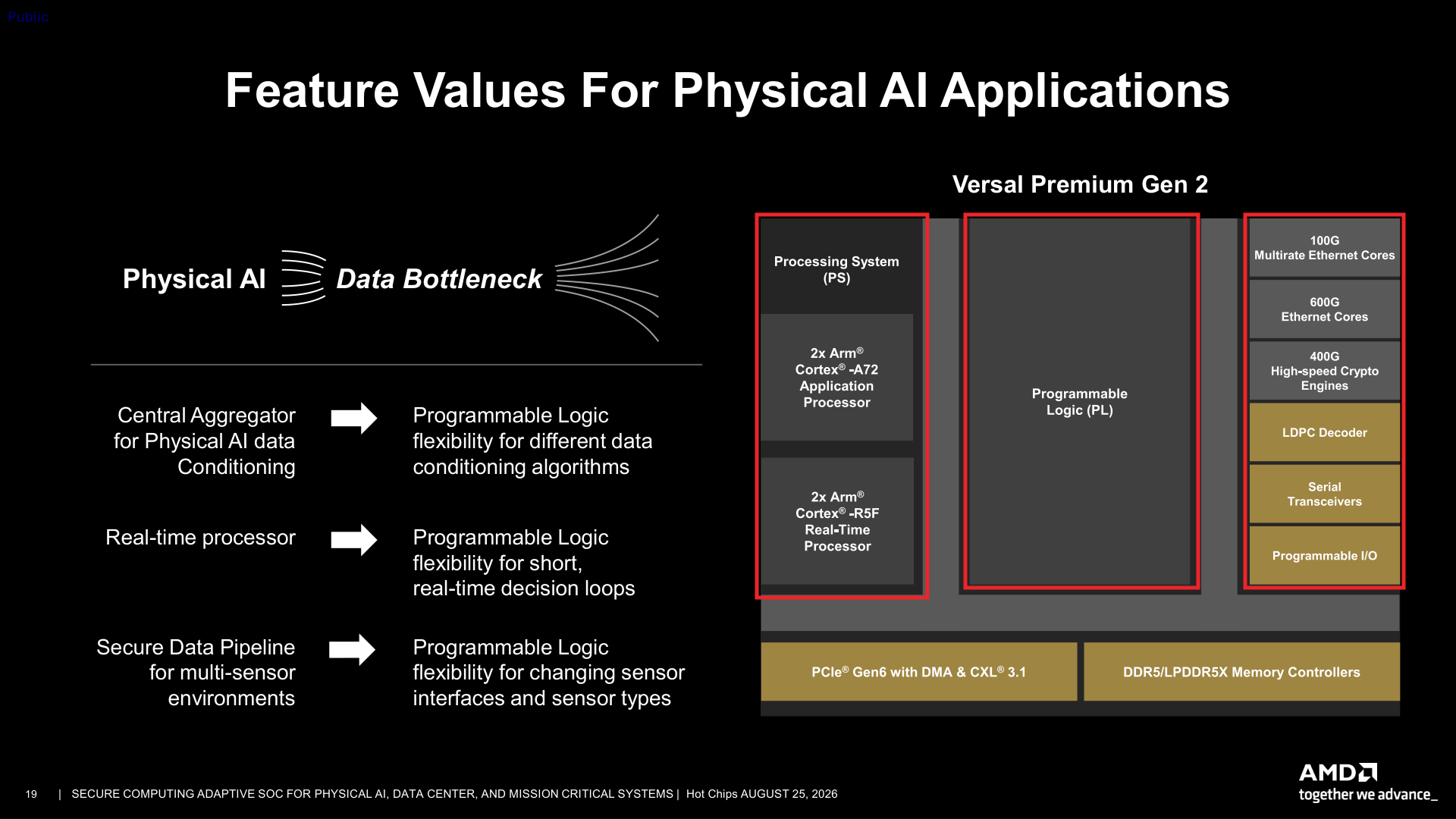
- Processors (left red box) use Arm (NASDAQ: ARM) Cortex-A72 cores for application software and Cortex-R5F cores for real-time control. AMD integrates this Arm processor IP with its programmable logic and communication engines.
- Programmable logic (central red box) implements custom circuits, such as a filter followed by a response stage.
- Communication blocks (right red box) combine protocol engines with transceivers and programmable I/O.
- A local circuit can therefore respond without sending every decision through application software.
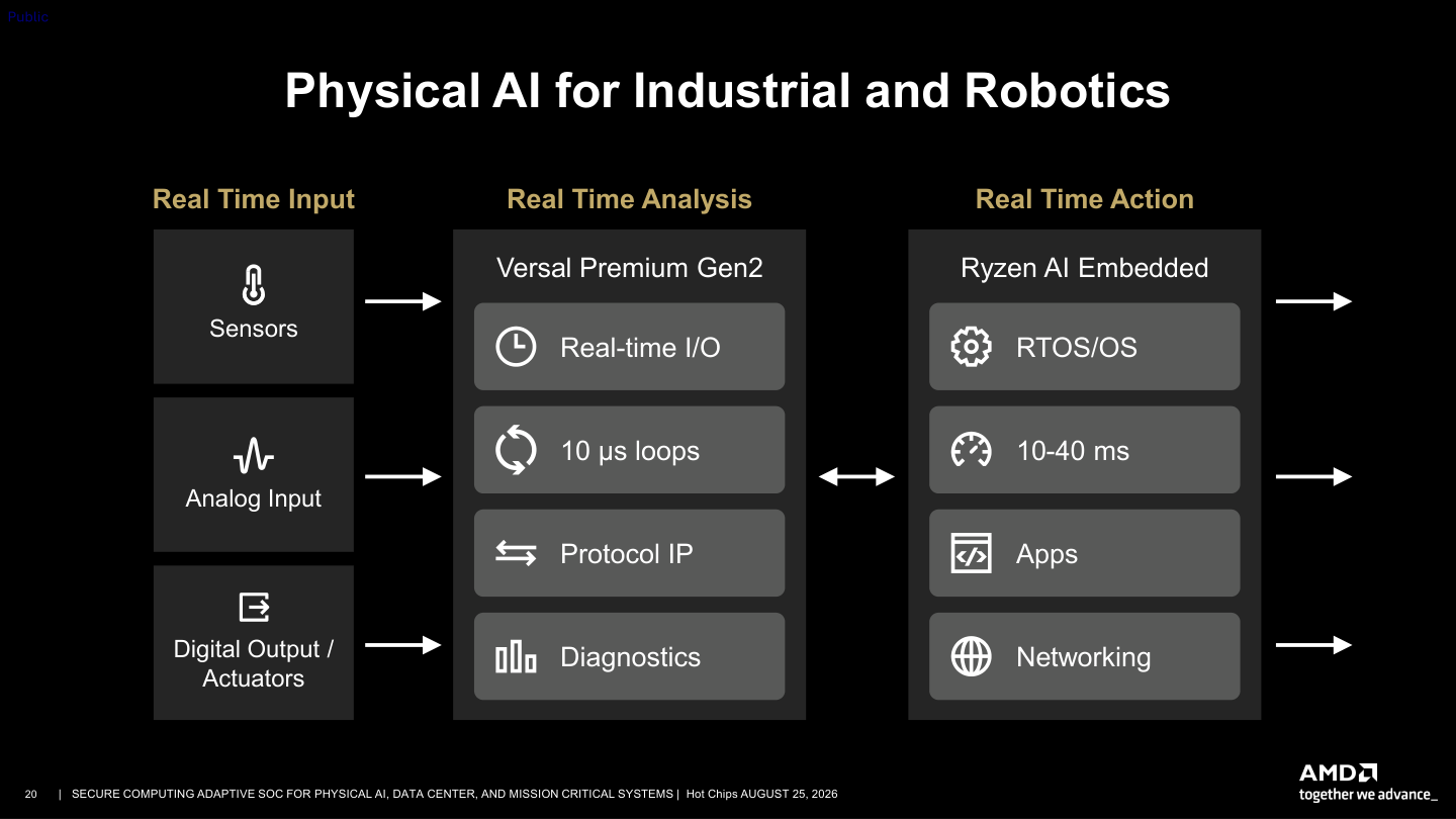
- The example separates a 10 μs local control loop from application work taking 10–40 ms. The local circuit keeps responding while software handles networking and broader decisions.
- This supports a role for programmable hardware in systems where predictable response matters more than a large average processing rate.
2) Integration saves board space but changes the development work
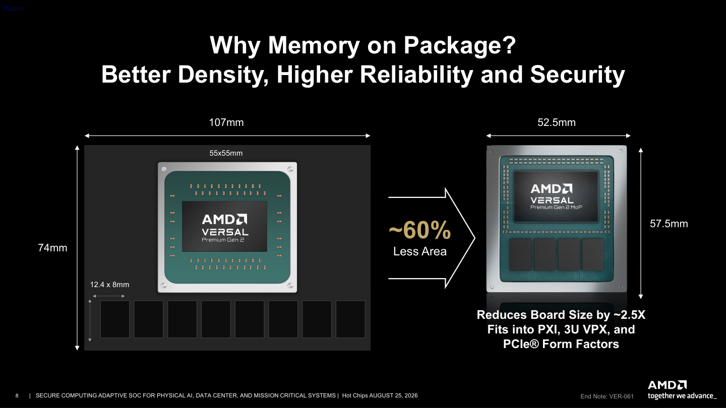
- Moving memory into the package reduces the illustrated processor-and-memory board footprint by about 60%. The relevant benefit is board space and routing inside a constrained enclosure, not a comparable increase in compute performance.
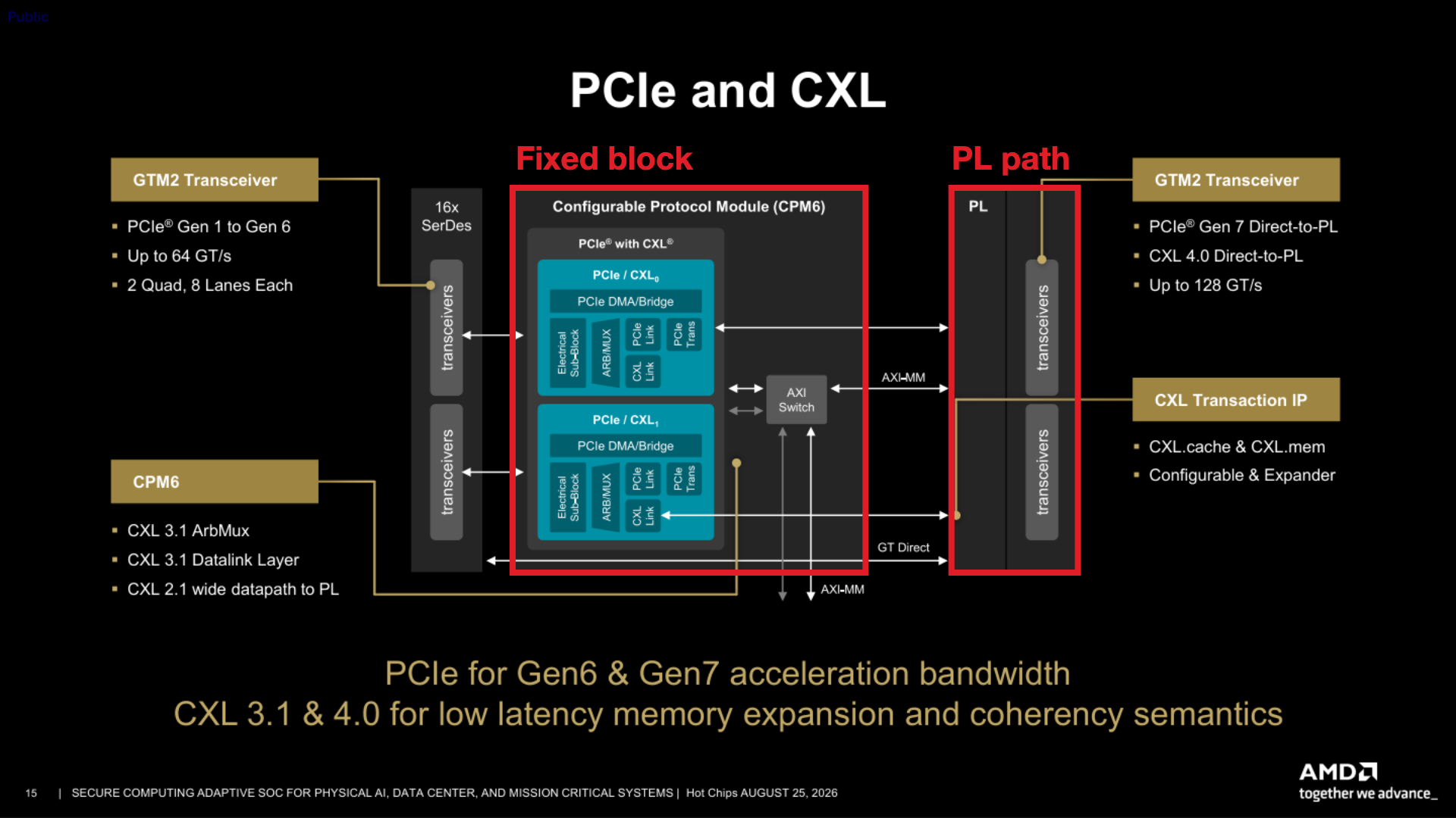
- The red rectangles identify two connection paths:
- The fixed PCIe / CXL module supplies implemented protocol functions.
- The programmable-logic path lets the developer build a different implementation, which also needs validation.
- Fixed circuits reduce customer-specific implementation work. Programmability preserves room to adapt. Custom logic also requires design and validation work.
(2) AMD Versal RF: remove unwanted data before it reaches the CPU or GPU
1) Spend local compute to save communication
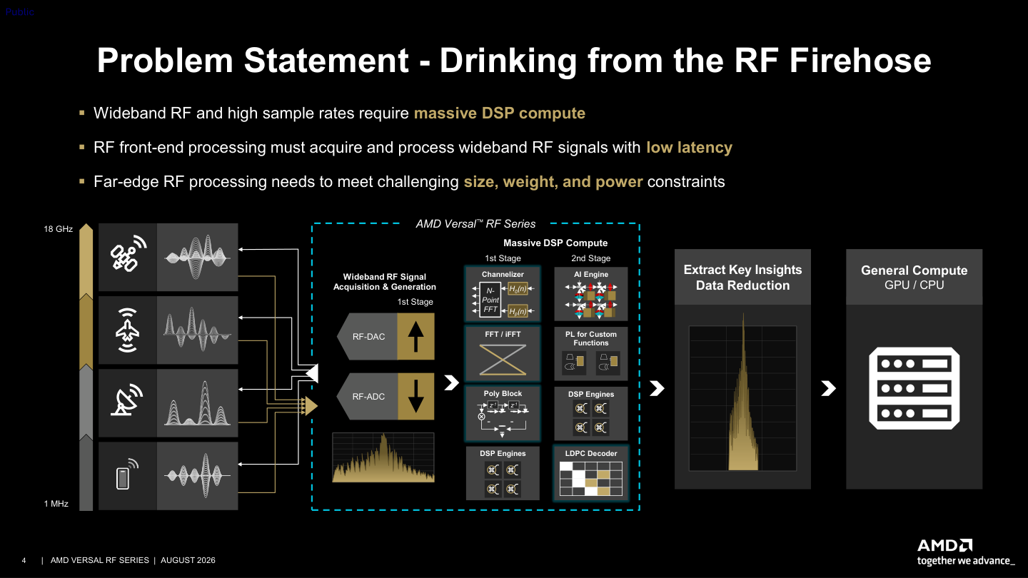
- The path runs from radio acquisition through local filtering to a reduced output. Dedicated circuits handle recurring operations, while programmable stages handle changing algorithms.
- Versal RF also uses Arm Cortex-A72 and Cortex-R5F processor cores for application and real-time software, alongside AMD’s RF and programmable processing blocks.
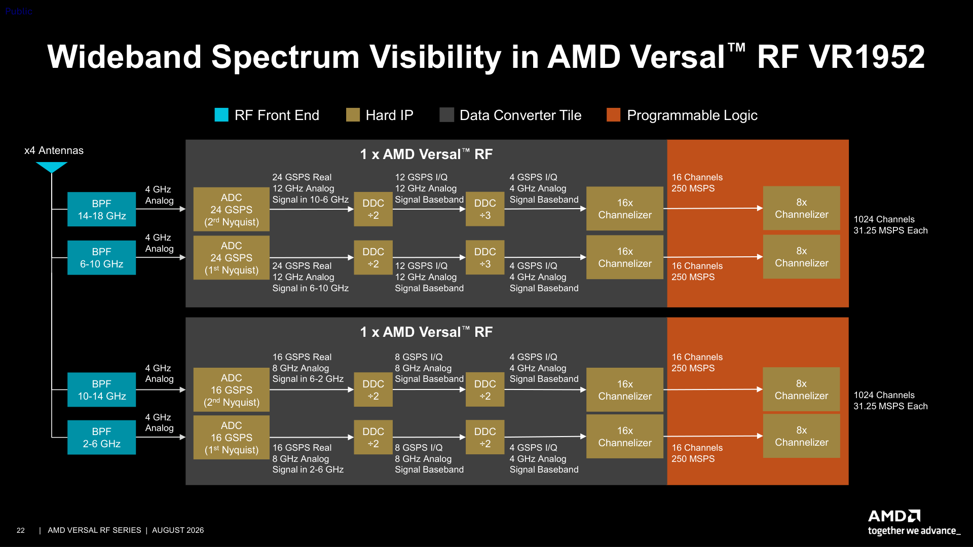
- The upper receive path starts with a 24 GSPS converter, meaning 24 billion samples per second. Downconversion shifts a selected frequency band for processing; filtering and channelization retain useful bands as smaller streams.
- The final 31.25 MSPS label describes one resulting stream, not the total system output. These are sample rates rather than byte rates.
- Removing unwanted samples locally reduces the bandwidth and power needed to export them. The reduction depends on how much of the raw stream the application can discard.
2) Use dedicated circuits for stable operations
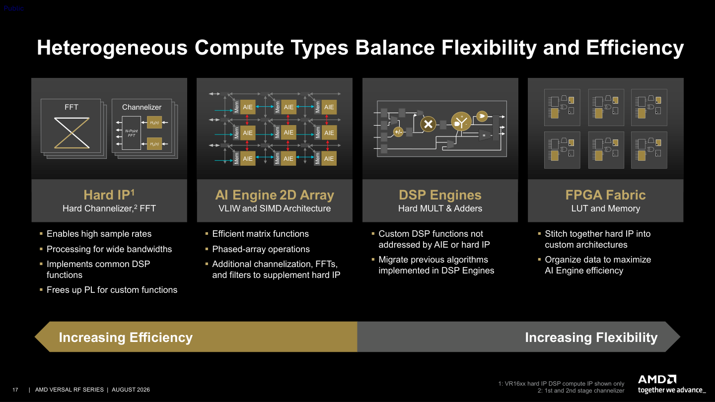
- The columns compare dedicated FFT / channelizer circuits with more programmable resources. An FFT separates a signal into frequency components; a channelizer divides its spectrum into bands.
- Dedicated circuits perform the recurring work efficiently and leave programmable resources for changing algorithms. Their narrower function becomes a limitation when the required operation changes.
- This is a route to specialization for customers who need some custom processing without designing a complete accelerator from scratch.
3) Local control can matter beyond data reduction
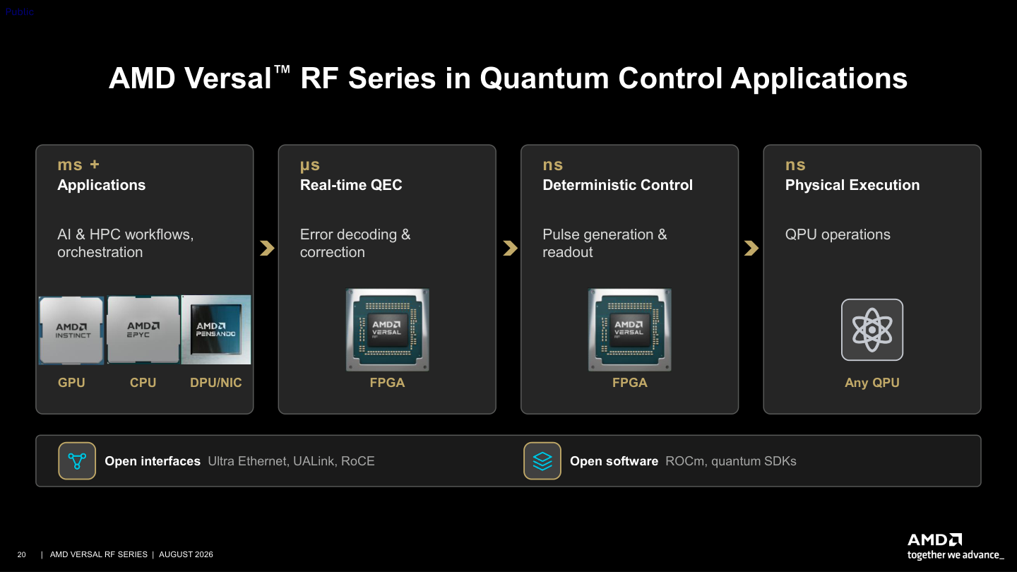
- The quantum-system example assigns millisecond orchestration, microsecond error decoding and nanosecond pulse control to different resources. The FPGA supports the classical control around quantum computation.
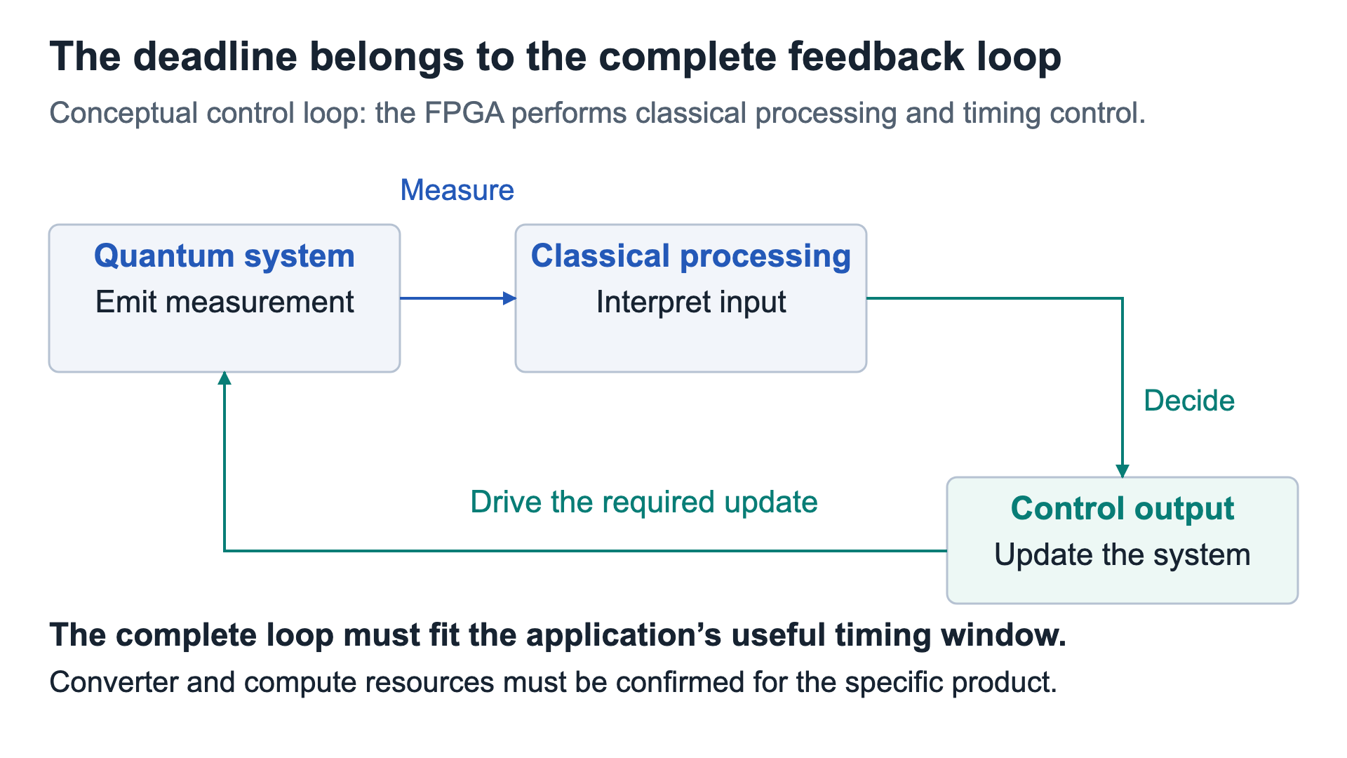
- Measurements must produce a control response while the quantum state remains useful.
- The local feedback path must meet the response deadline; higher peak throughput alone does not establish that it does.
2. Samsung and XCENA move computation toward stored data
(1) Samsung LPDDR5X-PIM: keep the repeated weight reads inside memory
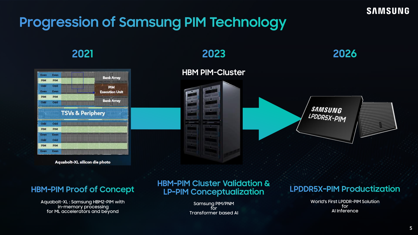
- The slide progresses from an HBM-PIM proof of concept through cluster validation to LPDDR5X-PIM productization in the presentation. Moving the approach to low-power memory aims to reach a wider range of inference systems.
1) Keep repeated weight reads inside memory
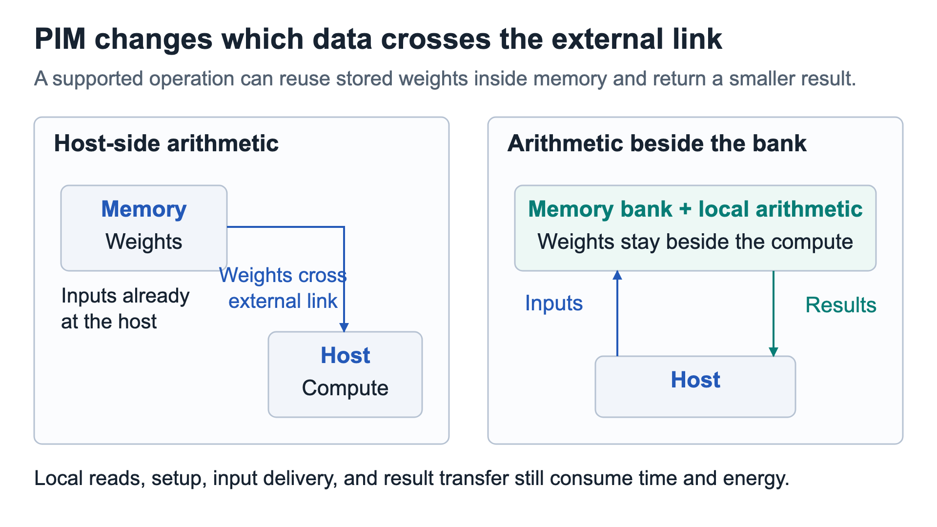
- The left path transfers weights to the host before calculation. On the right, processing in memory (PIM) performs selected arithmetic beside the stored weights and returns smaller results.
- Samsung Electronics (KRX: 005930) adds multiply-and-accumulate resources beside DRAM banks. The host supplies activations, which are the current calculation's inputs.
- Memory suppliers can reduce external traffic by supplying some of the calculation as well as storage. The reduction helps most when repeated weight reads limit execution.
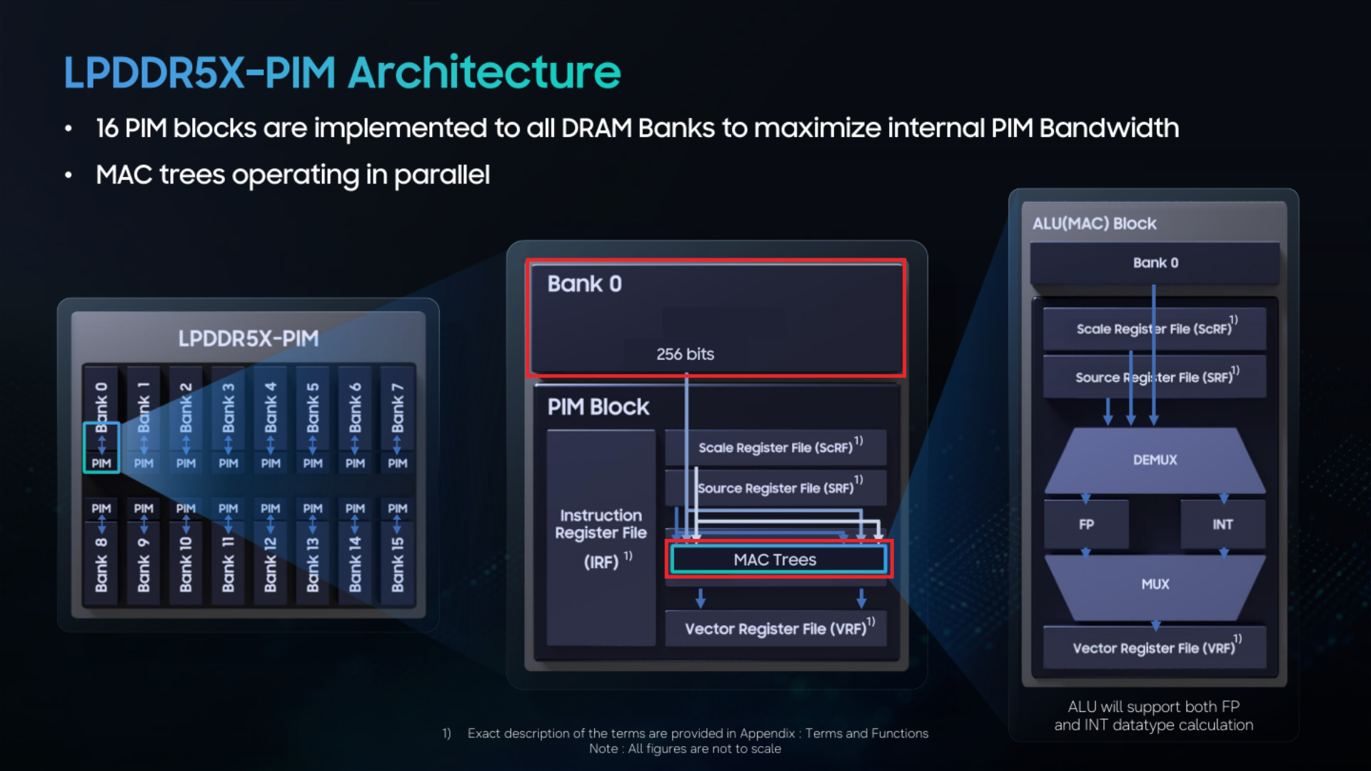
- In the enlarged bank, the upper red box marks stored weights in Bank 0. Those weights and input registers feed the multiply-and-accumulate trees in the lower red box. The vector registers hold the combined results for host readout.
- The internal PIM bandwidth describes parallel work inside memory. It does not widen the external pins; applications benefit only when their work can execute on that internal path.
2) Preserve operand identity and operation order
- Moving arithmetic into memory also changes the software's responsibility: a memory request now participates in a calculation, so it must select the correct input and wait until that input is ready.
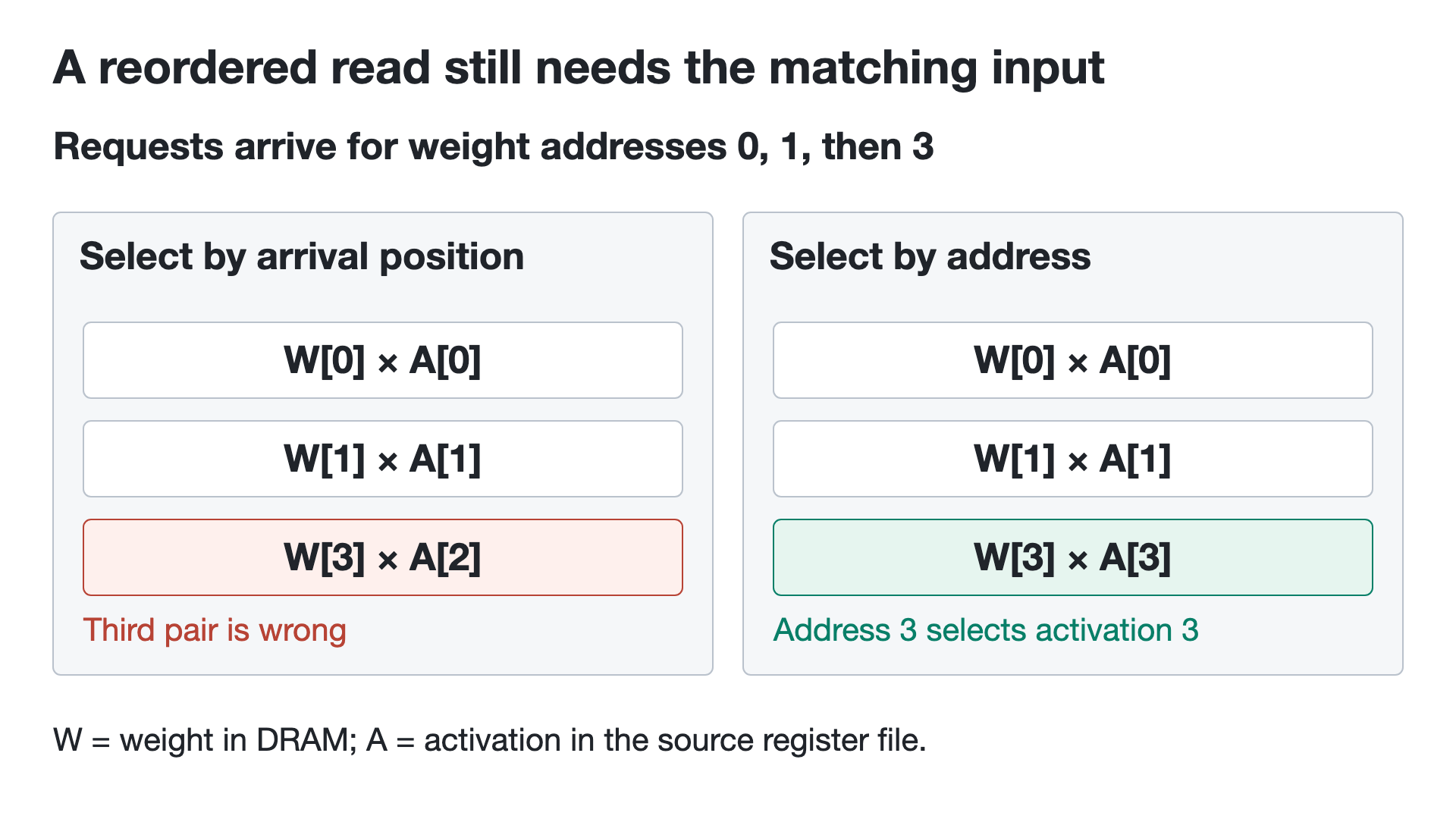
- The memory controller can reorder eligible requests to improve efficiency.
- Pairing inputs with weights by arrival order can then match the wrong values, as the incorrect path shows (left).
- The corrected path (right) identifies the input from the request's address, preserving the intended pairing.
- Software must also finish writing an input before dependent computation begins.
- PIM needs coordinated controller and software support; arithmetic beside DRAM alone does not make existing programs use it.
3) Interpret the application demonstration
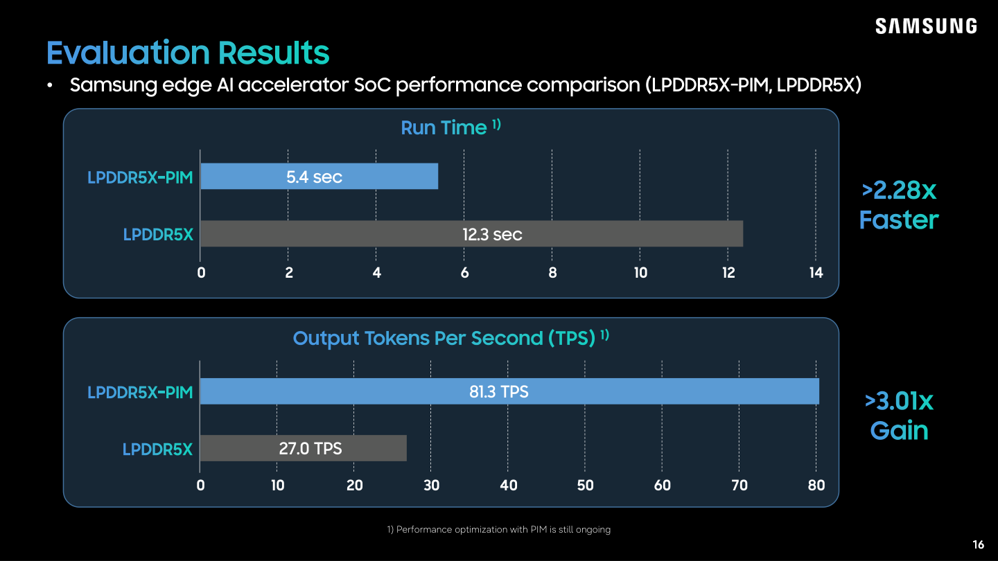
- The upper horizontal bars measure elapsed seconds, where shorter is better.
- The lower bars measure output tokens per second, where longer is better.
- Blue denotes PIM and gray ordinary LPDDR5X.
- In this demonstration, PIM reduces runtime from 12.3 to 5.4 seconds, about 2.28× faster, and raises output speed from 27.0 to 81.3 tokens/s, about 3.01×.
- Samsung tested Llama 3.1 8B on its edge AI accelerator SoC, with a stated 320-token input / output context and 8-bit activations, 4-bit weights and 32-bit outputs. These are results for that setup, rather than a general 3× gain for LPDDR workloads.
4) Translate the model into supported PIM operations
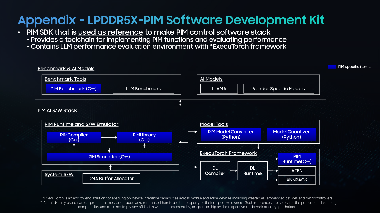
- The blue software blocks prepare PIM execution in stages:
- Convert the model into supported formats.
- Compile suitable operations for the memory-side arithmetic.
- Issue the required commands through the runtime.
- Existing programs need those additions before they can use PIM.
- Controller compatibility, model quality and software support determine whether internal bandwidth becomes a deployable advantage.
- Proposed LPDDR6-PIM standardization targets the mobile / client profile. The presentation does not establish broad adoption.
(2) XCENA MX1: process data beside memory and send back smaller results
- XCENA is a South Korean fabless semiconductor startup founded in 2022.
- Founded by semiconductor veterans from Samsung and SK hynix, it develops chips and software that expand memory capacity and process data near where it is stored.
- MX1 is a chip for a memory-expansion device that also performs selected calculations beside the stored data.
- The host is the main computer using the device. It connects to MX1 through CXL, a link that lets the computer access additional memory.
MX1 addresses two related problems:
- a) hold more data by combining DRAM with cheaper SSD capacity,
- b) reduce transfers by processing suitable work beside that data.
Extra capacity helps data fit. Local processing helps avoid repeatedly moving that data back to the host.
1) Process the data locally instead of sending everything to the host
The connection to the host can become the bottleneck
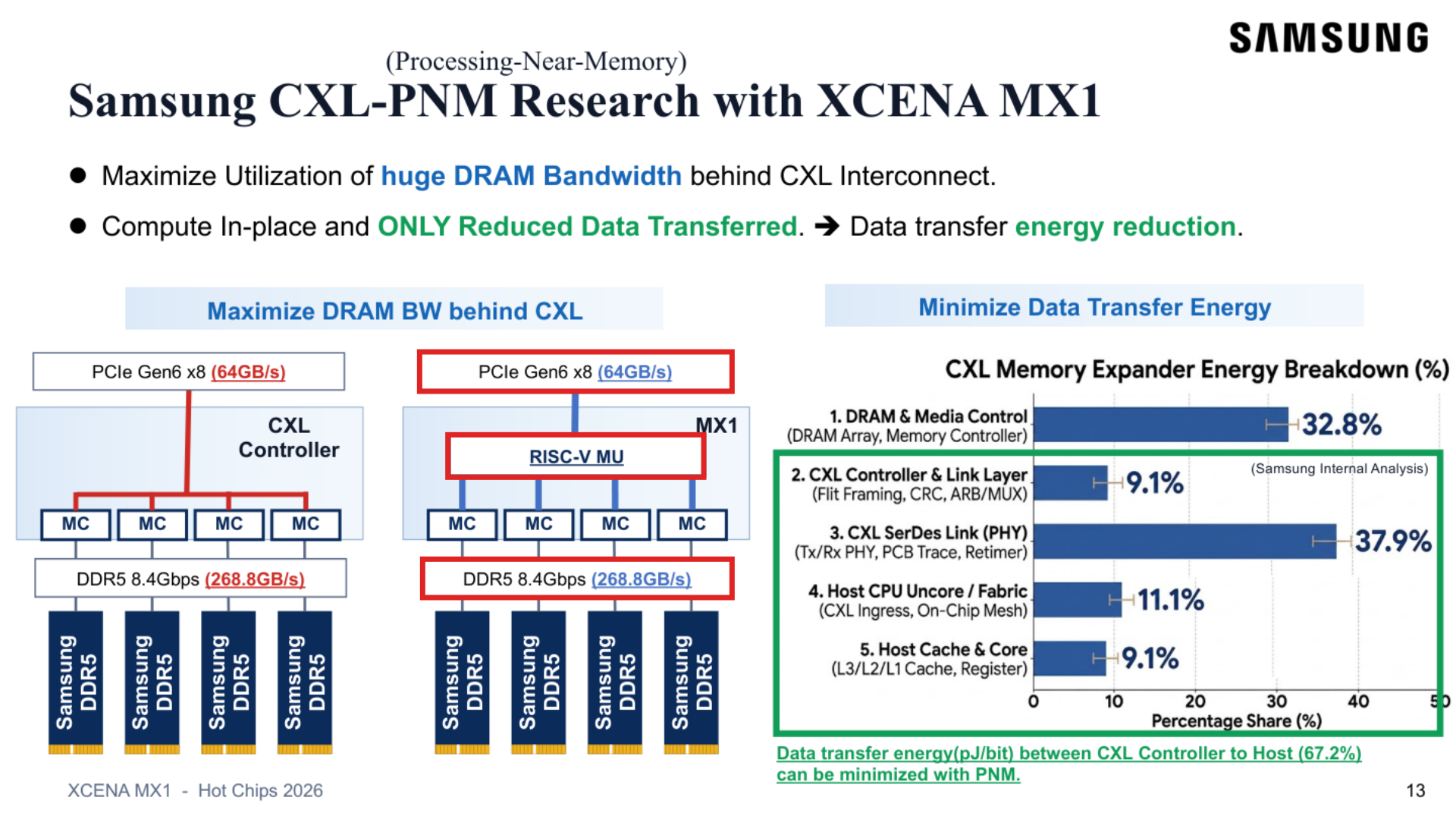
- The three red boxes locate local DRAM, MX1's processing unit, and the connection to the host.
- The DRAM provides 268.8 GB/s in the diagram, while the PCIe / CXL host connection provides 64 GB/s.
- If the host must receive all the raw data before processing it, that narrower connection limits delivery.
- MX1 can instead process suitable operations locally and send back their results.
A search example shows why this helps
- Imagine searching one million stored records for 1,000 matches. These are illustrative counts.
- With host-side processing, the records travel to the host for examination.
- With MX1, its local processors examine the records and return the matches.
- The benefit comes from transferring less data, without needing a faster host connection.
- The energy chart on the right supports the same motivation: it assigns 67.2% of the analyzed energy to the controller-to-host transfer path. That figure identifies a transfer-related cost.
Many small processors divide the job
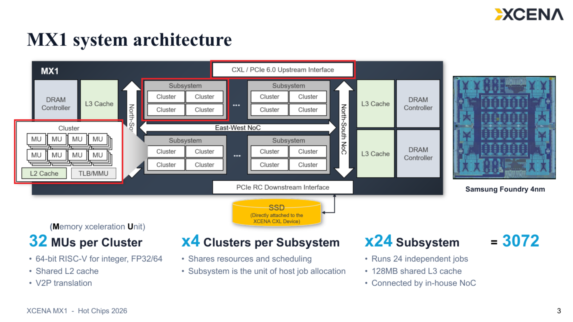
- The left red box enlarges a cluster, a group of small RISC-V processing cores.
- The central red box marks a subsystem, which groups clusters so software can assign them a job.
- The upper red box marks the CXL / PCIe upstream connection to the host CPU.
- For the record-search example, different groups can examine different portions of the records simultaneously.
- This works best when the portions are independent. If each record reveals where to find the next one, the search must follow that chain in order.
- Samsung Foundry manufactures MX1 on its 4 nm process, and Samsung DDR5 supplies the attached DRAM shown in the bandwidth diagram.
Software must arrange the local work
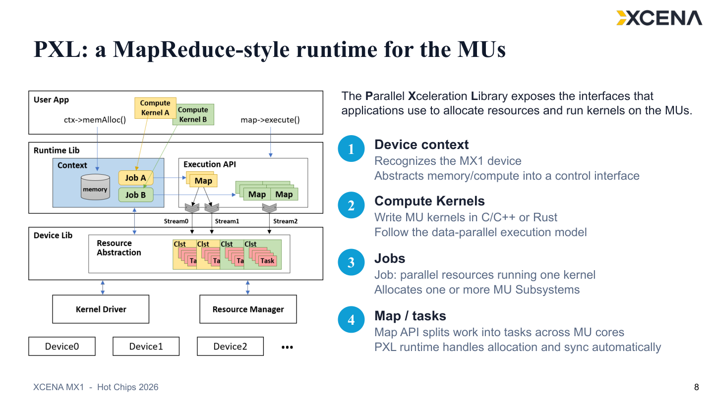
- Follow the diagram from the application at the top toward the devices at the bottom:
- The application requests a supported calculation.
- PXL, XCENA's runtime software, assigns processing groups to the job.
- It divides the job into tasks for local cores and coordinates completion.
- The host receives the results instead of reading every input itself.
- Samsung's Near Data Compute (NDC) API connects applications to device-specific software such as XCENA's library.
- Attaching MX1 does not automatically accelerate an existing program. Software must direct suitable work to the device.
- The presented PyTorch integration remains work in progress.
- Shared virtual addressing lets host and device code refer to the same data using the same addresses. This simplifies programming, but data still has a physical location and may need to move.
2) Use SSD capacity while keeping frequently needed data in DRAM
- MX1 can attach SSD storage and make its capacity accessible through the memory connection.
- SSD capacity costs less per byte than DRAM, but retrieving data from it takes longer.
- MX1 therefore uses DRAM as a cache: a faster holding area for data needed now or likely to be reused.
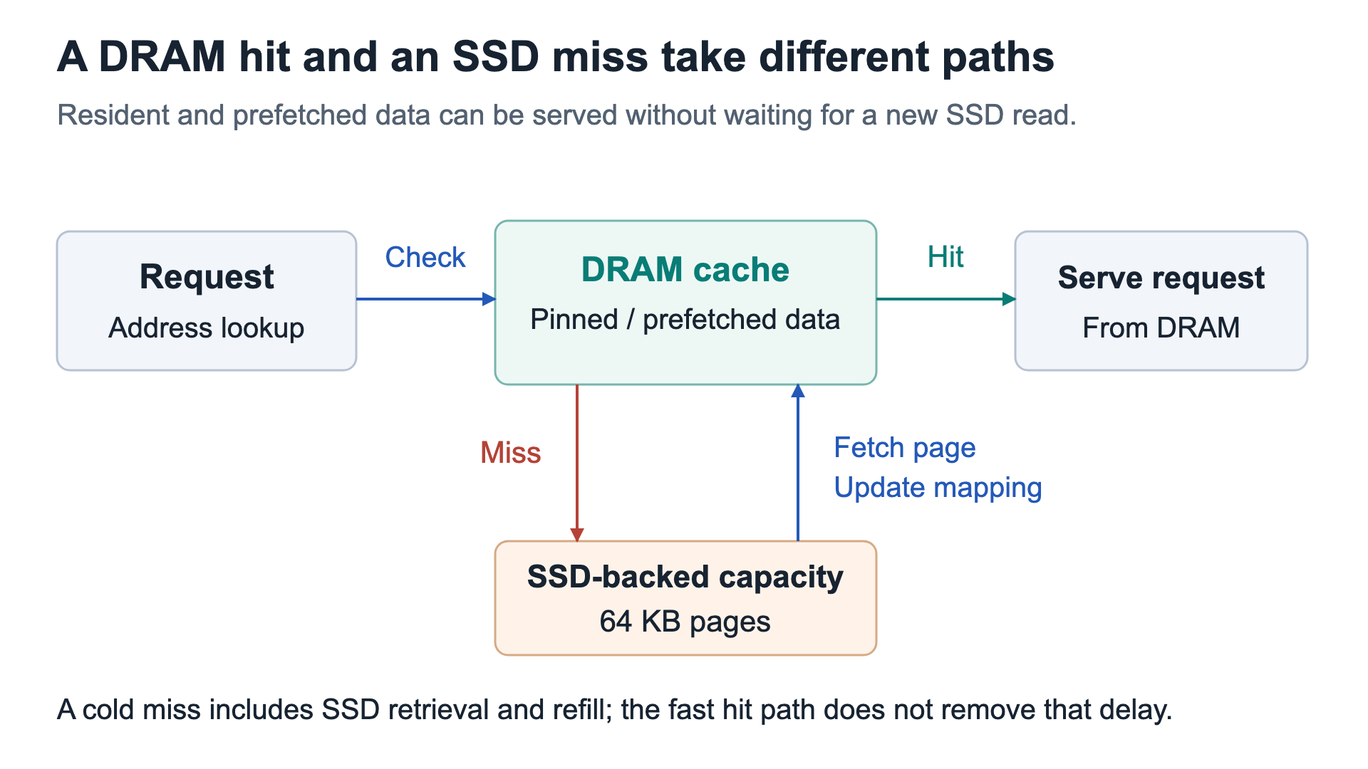
- Cache hit, green path: the requested data is already in DRAM, so MX1 can serve it from there.
- Cache miss, lower red path: the requested data is absent from DRAM.
- MX1 fetches the containing 64 KB block, called a page, from SSD.
- It places that page in DRAM and records where it is.
- The waiting request can then use the data.
- Software can reduce these waits in two ways:
- Pinning keeps selected data in DRAM because it is expected to be reused.
- Prefetching retrieves data before a request needs it.
- For example, several AI requests may share the same opening instructions or document. Keeping that shared prefix's cached state in DRAM avoids repeatedly fetching it from SSD.
- In the pinned-prefix demonstration, the first token arrived in 385 ms, compared with 340 ms for the DRAM reference.
- The system using SSD-backed capacity responded almost as quickly as the DRAM reference because the repeatedly needed data stayed in DRAM.
- The added capacity works best when frequently needed data stays in DRAM or arrives ahead of use. An unexpected SSD retrieval still adds waiting time.
3) Search a large database locally and return the closest matches
- A vector represents an item, such as a question or document, as a list of numbers. Vector search compares those numbers to find similar items.
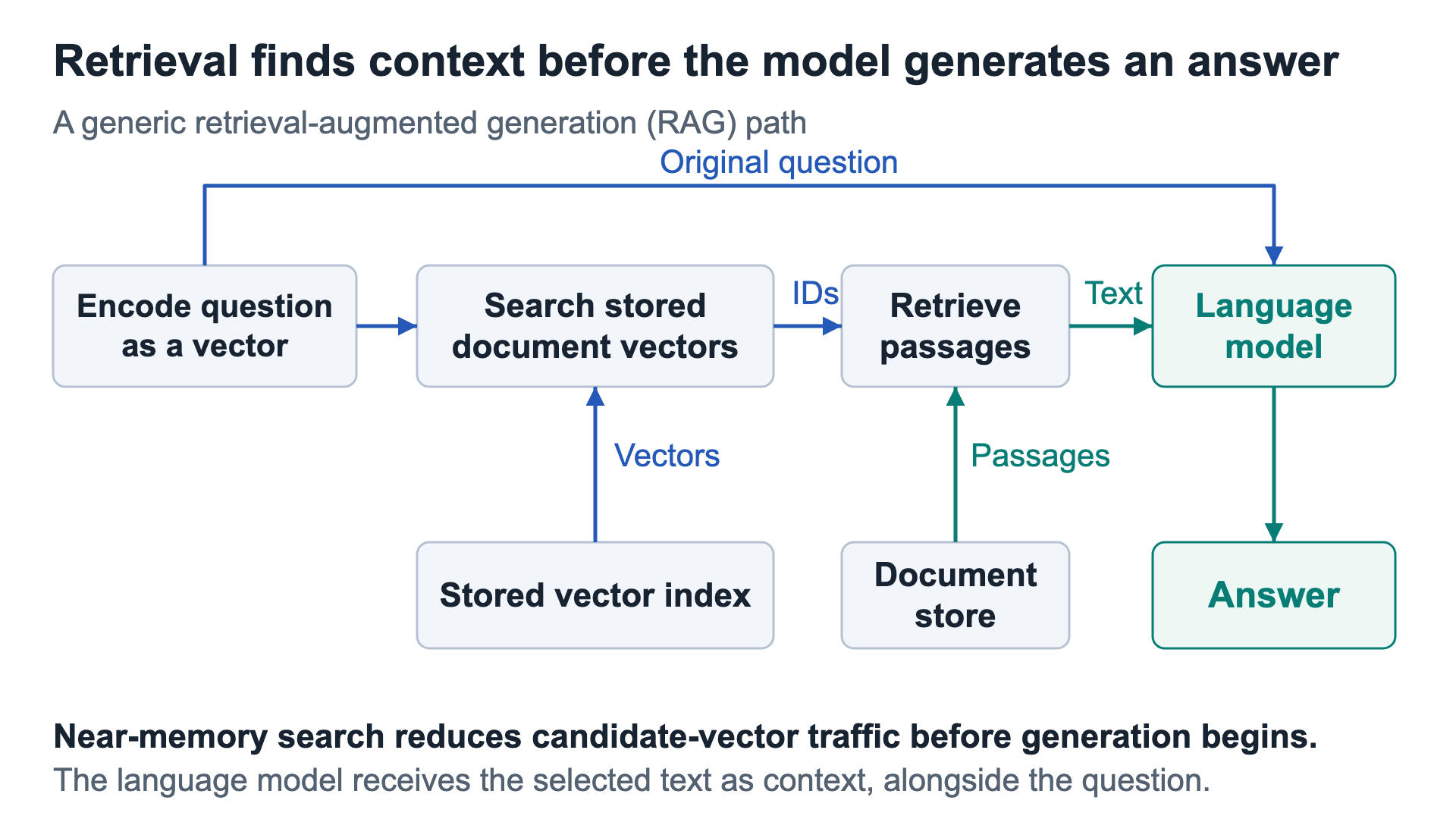
- In retrieval-augmented generation (RAG), the system:
- Converts the question into a search vector.
- Searches stored vectors for relevant documents.
- Retrieves passages from the matching documents.
- Gives those passages and the question to the language model.
- Finding a few useful passages may require examining a much larger collection of vectors. That search is the work MX1 moves closer to memory.
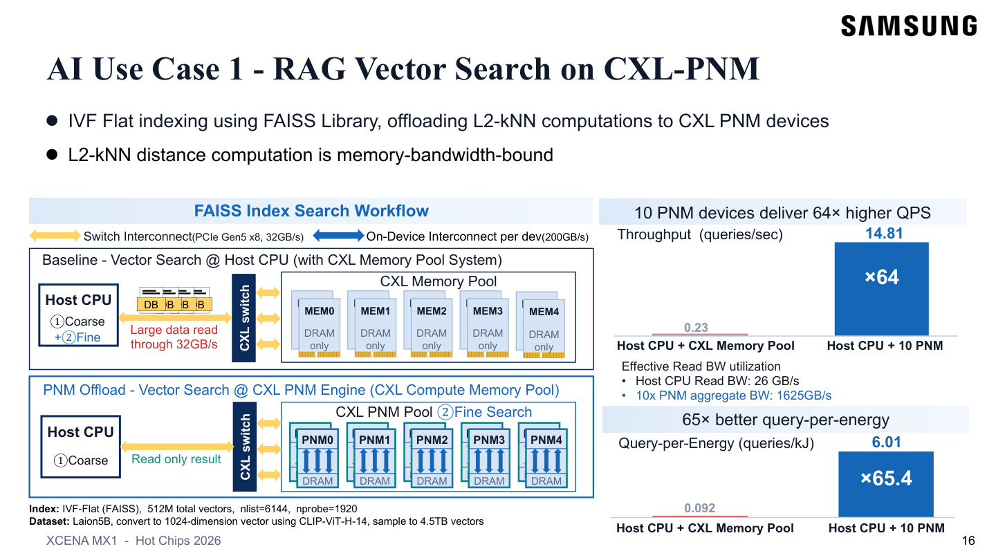
- Upper path, host-side search: candidate vectors cross the CXL connection so the host CPU can compare them with the query.
- Lower path, MX1 search: the work is divided:
- The host selects promising groups of vectors, narrowing the search.
- Memory-side processors compare the candidates within those groups.
- They return the closest matches rather than exporting all the candidates.
- Many local reads produce a small answer, reducing traffic through the host connection.
- The upper-right chart reports 0.23 queries/s for host-side search (gray) and 14.81 queries/s with ten PNM devices (blue) on the stated 4.5 TB vector dataset.
- The lower-right chart compares completed queries per kilojoule of energy; the PNM configuration also performs better on that measure.
- These results cover the search stage with the specified hardware. They do not measure the complete question-to-answer process.
4) Let the GPU and MX1 share attention work
The earlier Moving Bits article examined how KV-cache access connects memory capacity to network delays. MX1 addresses that transfer problem by computing beside remotely stored KV data.
- During text generation, the KV cache holds information about earlier tokens so the model can use that context again.
- Long conversations or documents make this cache larger. Some of it may need to reside outside the GPU's HBM.
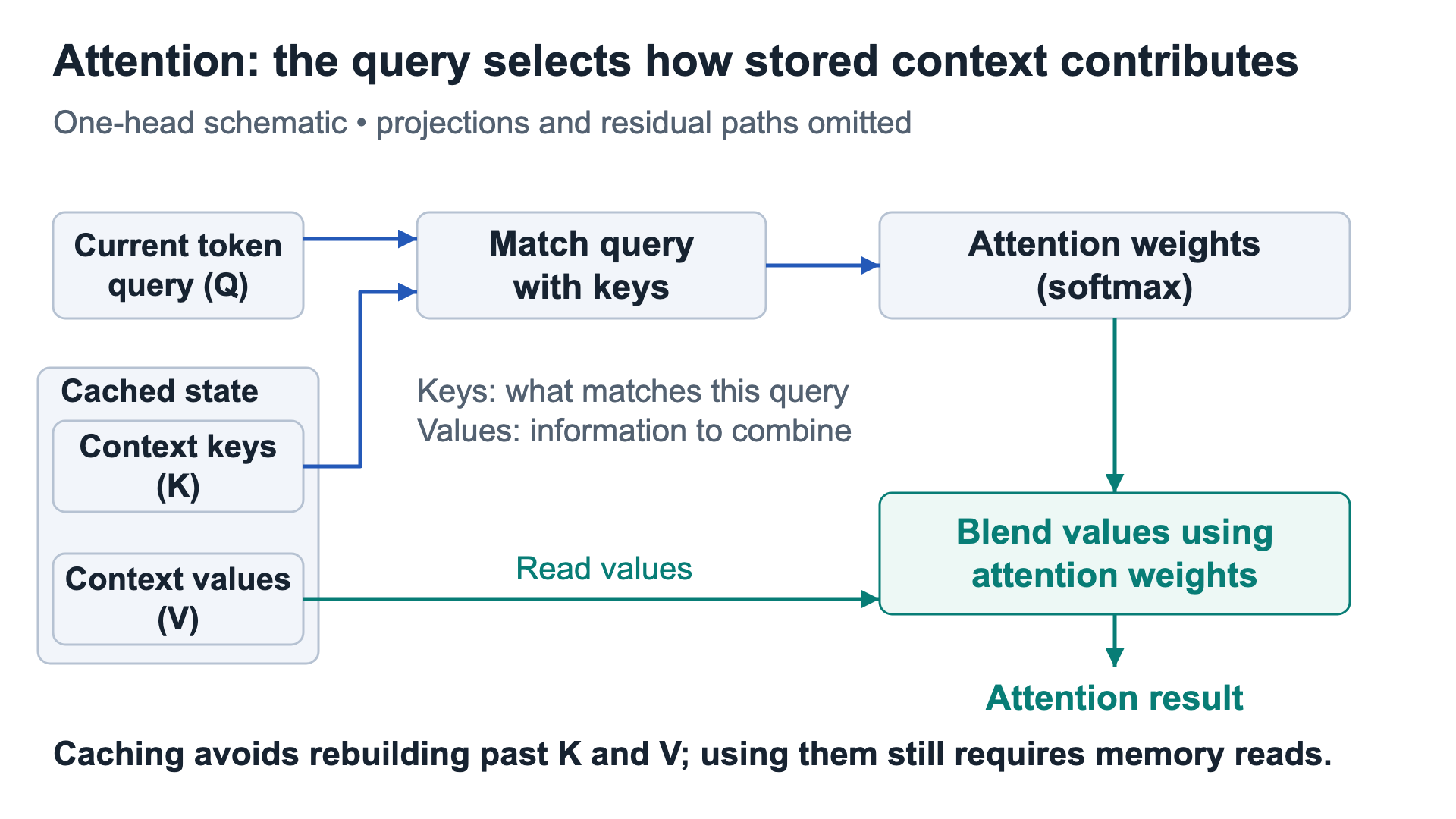
- Attention compares the current query with stored keys, then uses the resulting weights to combine stored values.
- If the needed keys and values sit in MX1-attached memory, the GPU could fetch them and do all the calculation itself.
- But moving those inputs can take longer than calculating with them.
- MX1 offers another route: calculate the remote data's contribution locally and send back the smaller partial result.
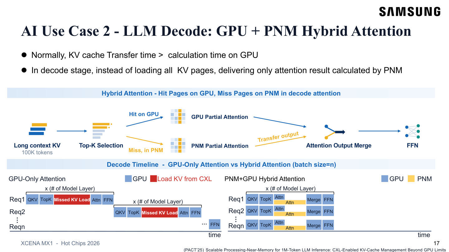
- Read the upper diagram from left to right:
- The selection step identifies the KV entries needed for this calculation.
- The blue path processes entries already held on the GPU.
- The yellow path processes the remaining selected entries beside their memory in the PNM device.
- The system combines both partial results into the attention output.
- In the lower-left timeline, the long red blocks show the GPU waiting for remote KV data to arrive.
- In the lower-right timeline, yellow PNM calculations overlap the blue GPU work, followed by a merge step.
- The goal is to move the smaller computed contribution instead of repeatedly moving the remote KV inputs. This helps when local calculation and result delivery cost less time than fetching those inputs.
5) Understand why several requests benefit more than one
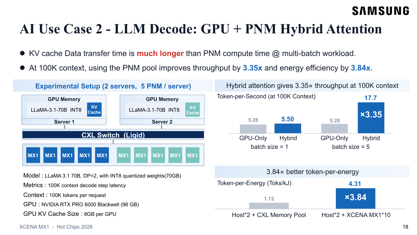
- The left setup uses two servers and ten MX1 devices connected through a Liqid CXL switch.
- The upper-right chart compares gray GPU-only bars with blue hybrid bars at a 100K-token context length:
- At batch size one, throughput changes only slightly: 5.28 to 5.50 tokens/s.
- At batch size five, the reported comparison is 5.28 to 17.7 tokens/s.
- Batch size is the number of requests handled together. More requests need more KV-cache space.
- When GPU memory cannot hold enough KV data, requests may have to wait their turn even if the GPU has spare arithmetic capacity.
- The MX1 memory pool holds additional KV data, while its processors calculate attention contributions beside that data.
- This lets more requests make progress together, which explains the larger gain in the multi-request test.
- The lower-right chart measures tokens produced per kilojoule of energy. Its improvement reflects the complete tested hybrid configuration, including the added devices.
- MX1 combines extra capacity with local processing to support more concurrent work. The result does not mean one isolated request becomes 3.35 times faster, and it includes the cost and power of additional hardware.
3. The network must deliver usable data and preserve progress
(1) Broadcom Thor Ultra: keep GPU data moving through a busy network
- Thor Ultra is Broadcom's (NASDAQ: AVGO) Ethernet network adapter, also called a NIC. It moves data between a server's memory and other machines on the network.
- When GPUs work together, one may need another's result before continuing. Delivering the required data correctly and on time reduces the wait before dependent GPU work can start.
1) Let the network adapter handle the repeated transfer work
- A buffer is an area of memory set aside to hold data, such as a GPU's partial calculation result.
- Remote Direct Memory Access (RDMA) lets network hardware transfer data between permitted memory buffers without making the CPU copy every byte through its own software.
- Software still sets up the transfer and memory permissions. The adapter handles the repeated data movement and reports completion.
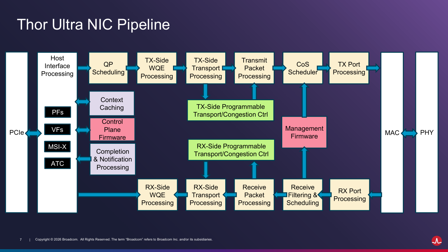
- The diagram separates sending from receiving:
- Upper path, left to right: accept a transfer request, divide its data into network packets, and send them out.
- Lower path, right to left: receive packets, check and place their data, then report completion to the host.
- Green blocks: programmable controls adjust how traffic is sent and respond when the network becomes congested.
- A packet carries a portion of the data, called its payload, plus a header containing delivery information. A large transfer usually needs many packets.
- Moving this routine work into the NIC frees CPU resources. The GPU still waits until the data it needs has arrived and is ready to use.
2) Use several paths, then put the arriving pieces in the right places
Several paths can reduce waiting behind a busy route
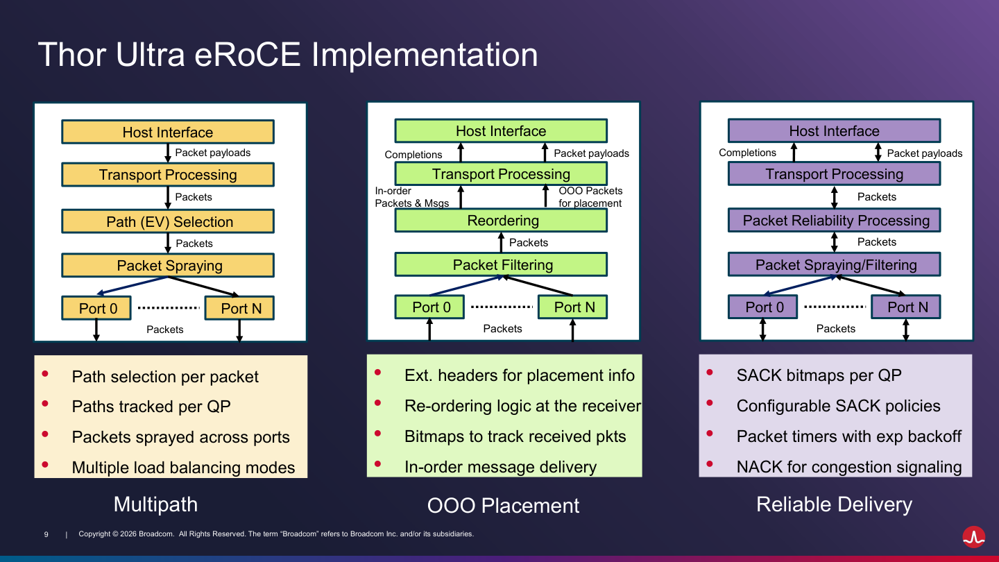
- If all packets from a transfer follow one busy route, they can queue there while another route has spare capacity.
- Packet spraying spreads packets across available routes. This gives the transfer more opportunities to make progress.
- Different routes can take different amounts of time, so the packets may arrive in a different order from the one in which they were sent.
- The slide assigns three jobs to the NIC:
- Yellow column: choose paths and send packets.
- Green column: use placement information to put arriving data in the correct memory locations and track what has arrived.
- Purple column: identify missing packets and arrange recovery.
Arrival order does not have to become data order
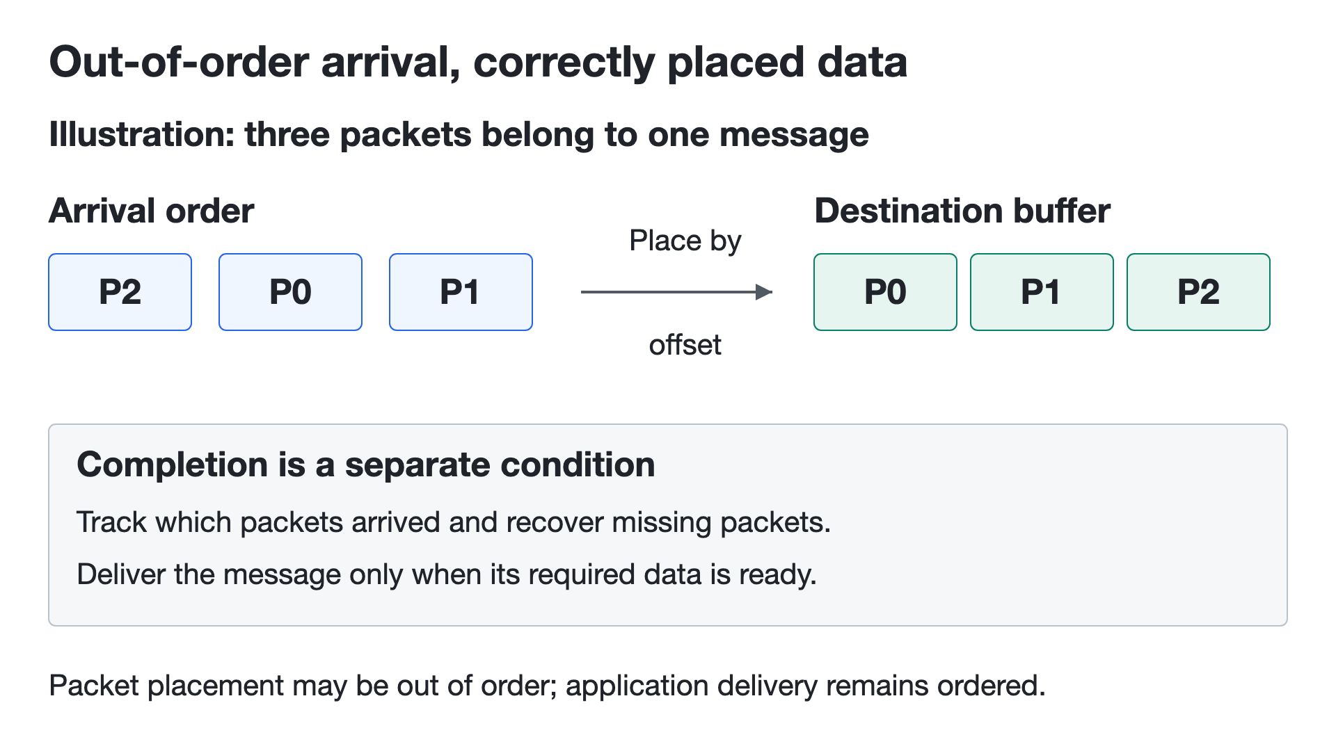
- Imagine a transfer divided into packets 0, 1, and 2, which arrive as 2, 0, and 1.
- Packet 2's placement information tells the receiver where its data belongs, so it can be written into the third part of the destination buffer immediately.
- Packet 0 fills the first part, and packet 1 fills the second.
- Placing packet 2 correctly does not mean the entire transfer is complete. The receiver must also track whether packets 0 and 1 have arrived.
- Software can release dependent GPU work after the required data and completion conditions are satisfied.
- The network can use several routes without forcing the application to consume incomplete or scrambled data.
3) Pace senders so they do not overwhelm the receiver
Credits grant permission to send
- Several GPUs may send results to the same destination at once. Even fast links cannot prevent a queue if data arrives faster than the destination can accept it.
- Receiver credits tell each sender how much data it is currently allowed to send.
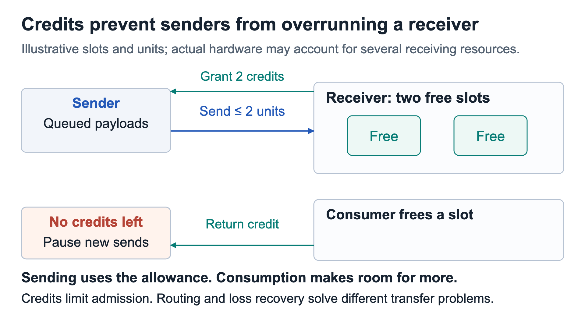
- The diagram uses two receiving slots as a simplified example:
- The receiver grants permission for two chunks of data.
- Sending those chunks uses the allowance.
- The sender waits for further permission instead of continuing without a limit.
- As receiving resources become available again, the receiver grants more credits.
- This coordinates multiple senders around the destination's available resources. The receiver can adjust allowances as congestion changes.
- Thor Ultra also permits a limited initial allowance, so a small transfer can start without waiting for a new credit exchange.
A lost packet still needs to be recovered
- Packet trimming provides an earlier signal that a packet's data was dropped.
- A supporting switch removes the payload but forwards the smaller header to the receiver.
- The receiver notifies the sender, which can adjust its sending rate and recover the missing data.
- Credits help control incoming traffic, while loss notifications help recover when delivery still fails. Neither makes an incomplete transfer ready for the GPU.
4) Stop one workload from taking all the shared network capacity
- A server may run several jobs through one physical NIC. Giving each job access to the adapter does not guarantee that they receive a useful share of its bandwidth.
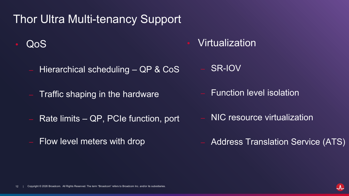
- The slide's left column, quality of service (QoS), controls how traffic shares the adapter:
- Scheduling chooses which waiting traffic is sent next.
- Rate limits cap the sending rate for a connection or workload.
- Hardware applies those rules without asking the CPU to make every packet-level decision.
- For example, a large background transfer could otherwise keep delaying another job's small messages. Scheduling and rate limits give the operator a way to control that competition.
- The right column, virtualization, lets workloads receive separately assigned NIC resources, called virtual functions, while sharing the physical adapter.
- Virtualization separates the assigned resources. Scheduling controls how their traffic competes for the shared link. Both matter when several jobs use the same server.
5) Understand why a fast link helps large transfers more than tiny messages
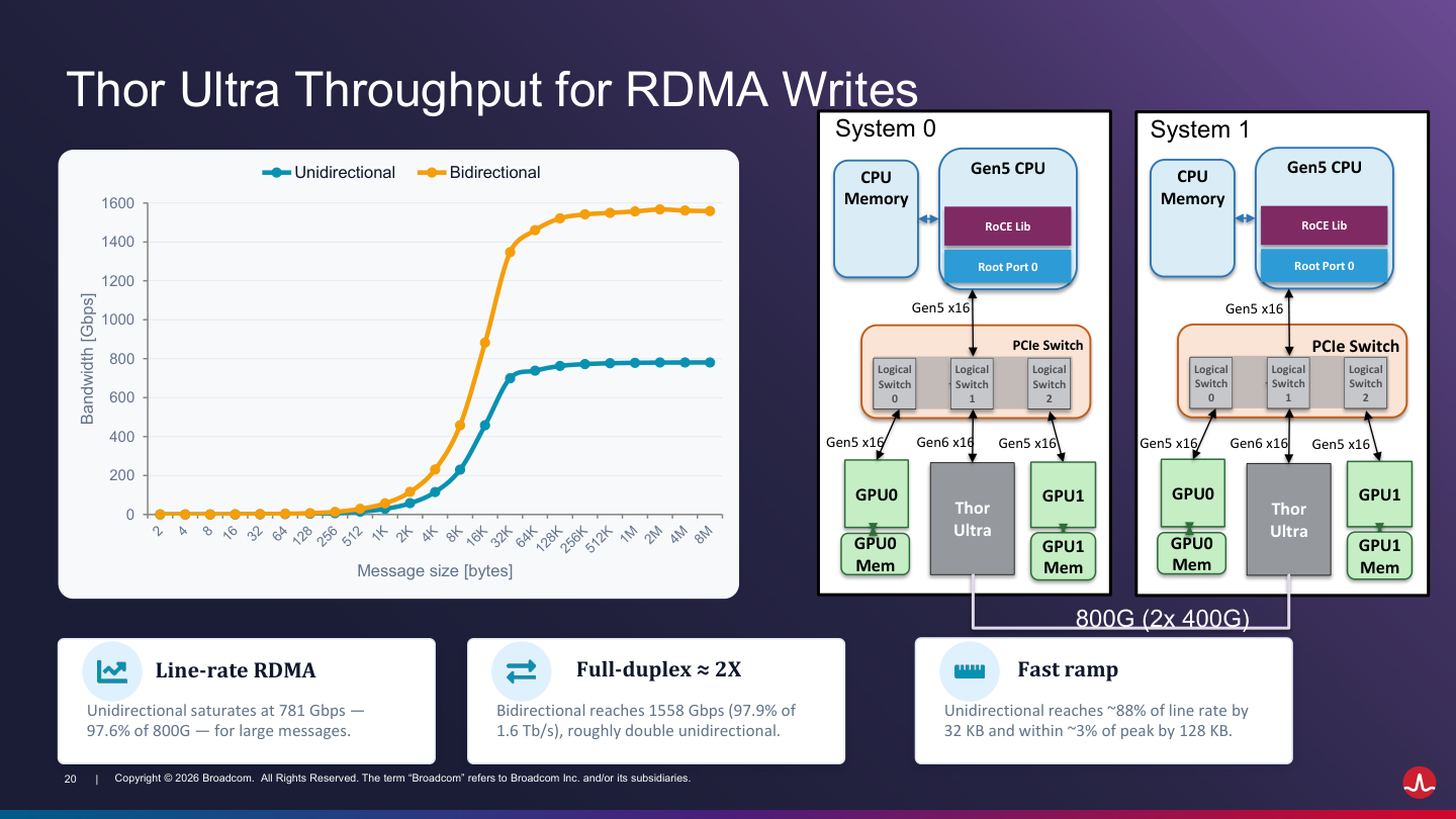
- The right-hand test setup connects two GPU-equipped systems through two 400G links, providing 800 Gb/s of network capacity in each direction.
- Read the graph on the left:
- The horizontal axis is message size in bytes, increasing in doubling steps.
- The vertical axis is bandwidth in Gb/s, or gigabits per second.
- The blue curve measures one-way traffic and approaches 800 Gb/s for larger messages.
- The orange curve adds simultaneous sending and receiving, approaching 1,600 Gb/s combined. It does not show 1,600 Gb/s in one direction.
A simplified way to think about the total is: time until usable ≈ handling time + waiting time + data transmission time + completion reporting.
- A faster link reduces the time spent transmitting data, but an exchange also takes time to process, wait its turn, and confirm that the data is ready to use. For a small message, those other delays can dominate.
- For a large transfer, transmitting all the bytes takes substantial time, so increasing bandwidth can significantly shorten the transfer.
- For a small message, transmitting its few bytes already takes very little time. A faster link saves little if the message still waits for processing, permission to send, or other traffic.
How the preceding transfer controls help
- Packet spraying uses multiple routes to reduce waiting behind a busy route.
- Receiver credits regulate incoming traffic so senders do not overwhelm the receiver. The limited initial allowance lets a small transfer start without waiting for a new credit exchange.
- Scheduling and rate limits control competition between jobs sharing the adapter.
- Placement, recovery, and completion tracking put received data where it belongs, recover missing pieces, and establish when dependent GPU work can proceed.
- Thor Ultra combines high data capacity with transfer management to keep GPUs supplied with usable data. The graph illustrates how achieved bandwidth changes with message size; it does not isolate how much each control improves small-message latency.
(2) NVIDIA BlueField-4: separate infrastructure ownership from tenant execution
The roles of BlueField-4 and ConnectX-9 within the platform were introduced in Vera Rubin Decoded, Part 3. Here, the focus is how they divide infrastructure control and data transfers.
1) Separate tenant and provider control
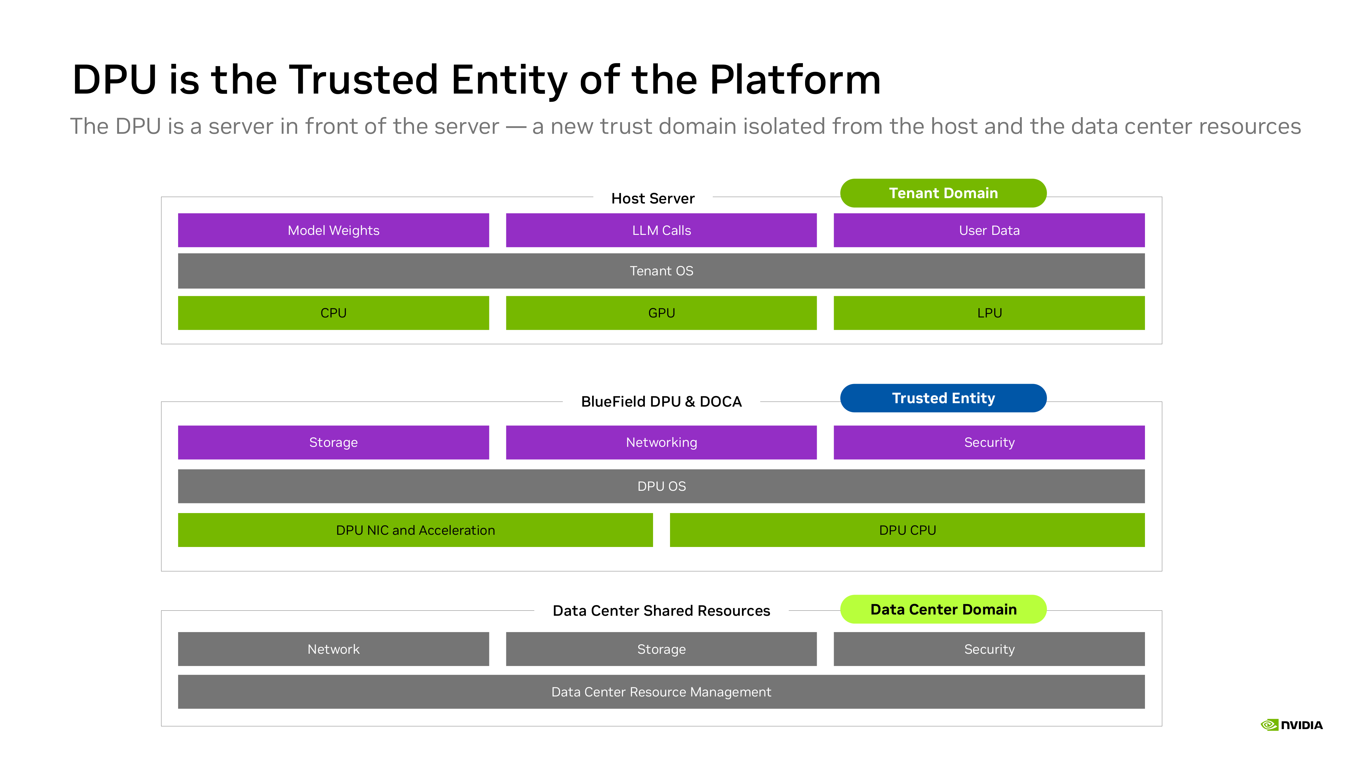
- The upper stack contains the customer's workload and operating system, while the middle DPU stack runs infrastructure services under the provider's control.
- The separation matters when a customer needs administrator access to its own OS: that access should not also let it rewrite the provider's storage or network policy.
- Shared data-center resources remain below those domains. The DPU enforces the provider's controls across those domains.
- NVIDIA (NASDAQ: NVDA) implements that provider-controlled domain in BlueField-4, a data processing unit (DPU) combining a CPU with network, storage, and security acceleration.
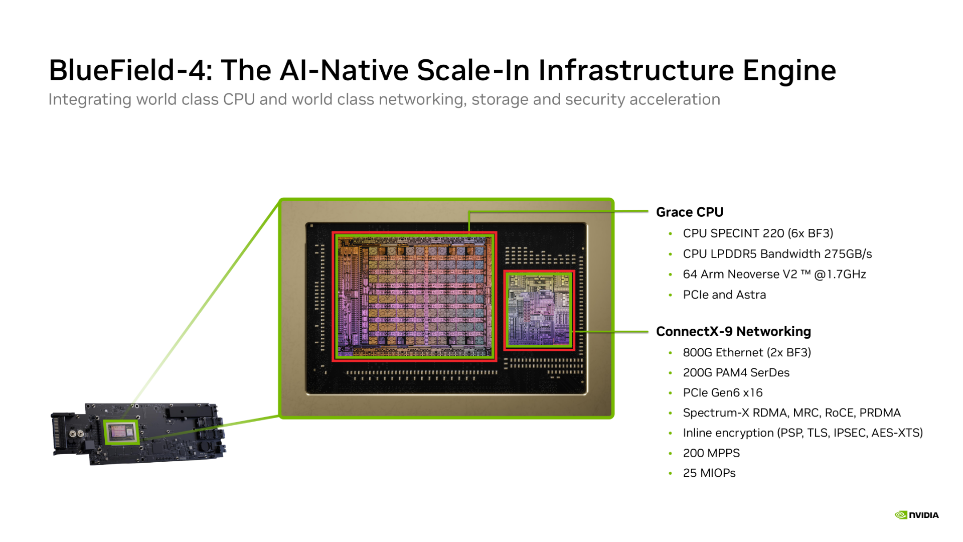
- The Grace CPU in the larger left red box uses Arm Neoverse V2 cores to run changing control tasks, such as session keys, storage volumes and health monitoring. NVIDIA supplies the Grace design, integrating Arm’s CPU core IP.
- ConnectX-9 in the smaller right red box handles recurring transfers, packet processing and inline protection.
- The provider retains software control of policy while hardware performs the repeated data-path work.
2) Manage distributed NICs without relaying every byte
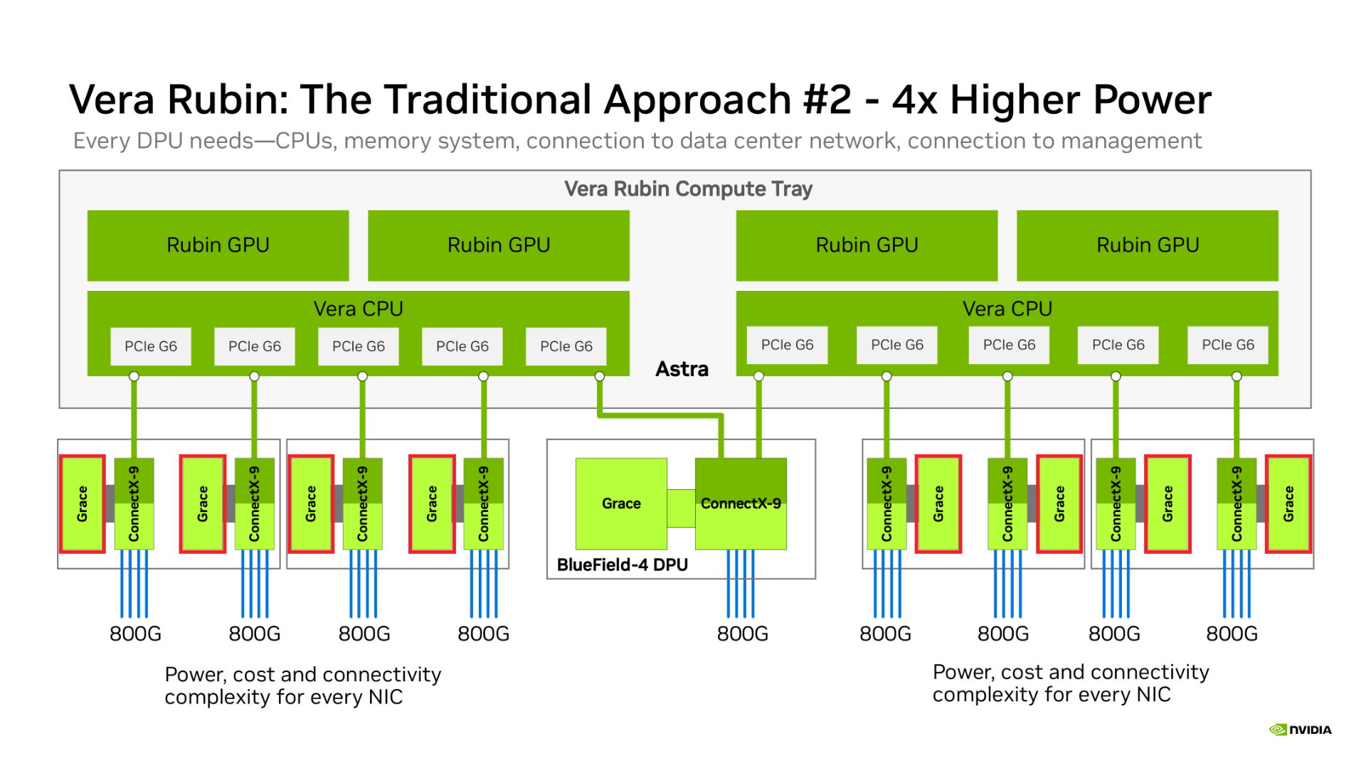
- A tray with many fast NICs creates a scaling problem. Attaching a complete DPU to each NIC repeats its CPU, memory, and management connections. Leaving those NICs under tenant control instead weakens the intended provider-controlled boundary.
- Astra addresses this by letting one DPU manage distributed NIC resources. The next diagram keeps the direct GPU data paths while adding the separate provider-management connections.
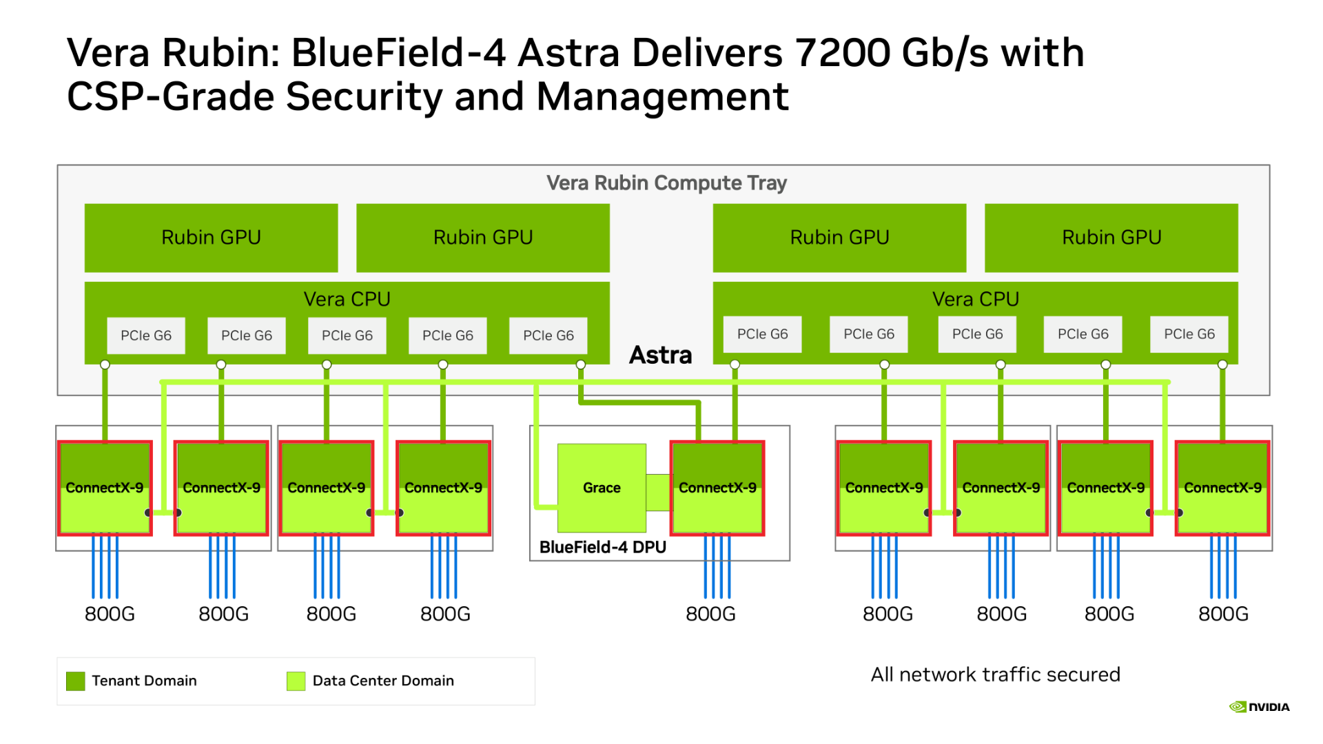
- The eight external ConnectX-9 blocks keep their direct payload paths.
- Dark green marks tenant resources. The light-green Astra path lets the provider configure and supervise devices separately.
- One DPU can manage several NICs without relaying all their bytes through its CPU cores.
- Consolidating management can therefore avoid repeating a full DPU's CPU, memory and management resources at every NIC.
3) Place context according to urgency and reuse
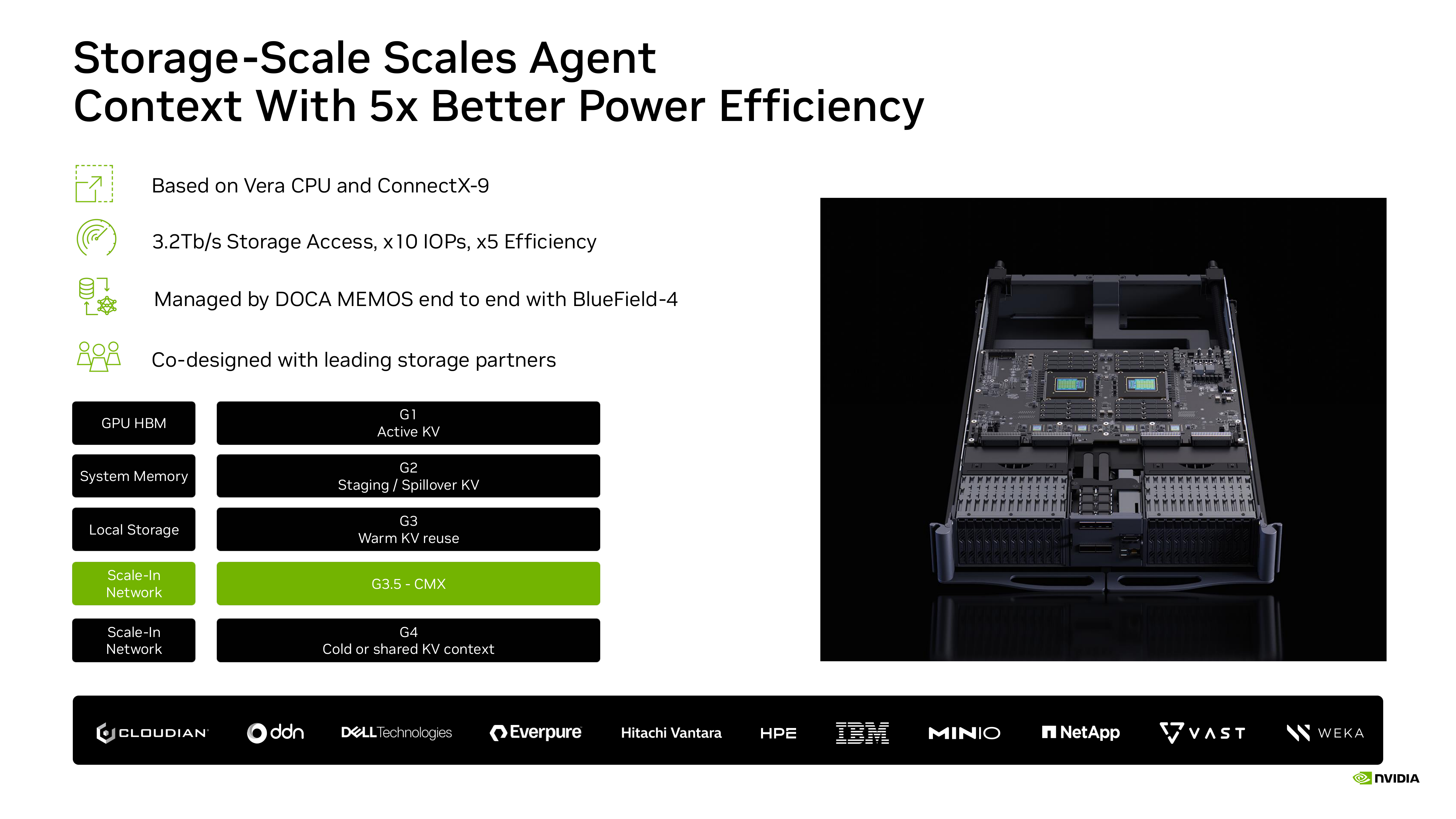
- The lower-left hierarchy places KV attention state according to when it will be needed again, reserving the nearest memory for the most urgent reads.
- G1 is GPU HBM, where active context can feed the current attention calculation.
- G2 is system memory, which can hold overflow and stage likely future inputs before they are needed in HBM.
- The wider local and network tiers, including the green G3.5 row, retain context for reuse or sharing without occupying the same scarce GPU space.
- A page in a farther tier adds a retrieval step before attention can use it. The tier names identify placement roles, not interchangeable access speeds.
- Active pages stay close because repeated distant retrieval would delay generation. Staging moves likely future pages before they become urgent, while colder tiers retain less-active state.
- Infrastructure processors manage placement and retrieval around the GPU. Moving less-active state out of HBM saves space, provided required pages return before their retrieval delays the response.
(3) NVIDIA Spectrum-X: control interference and recover without losing the whole job
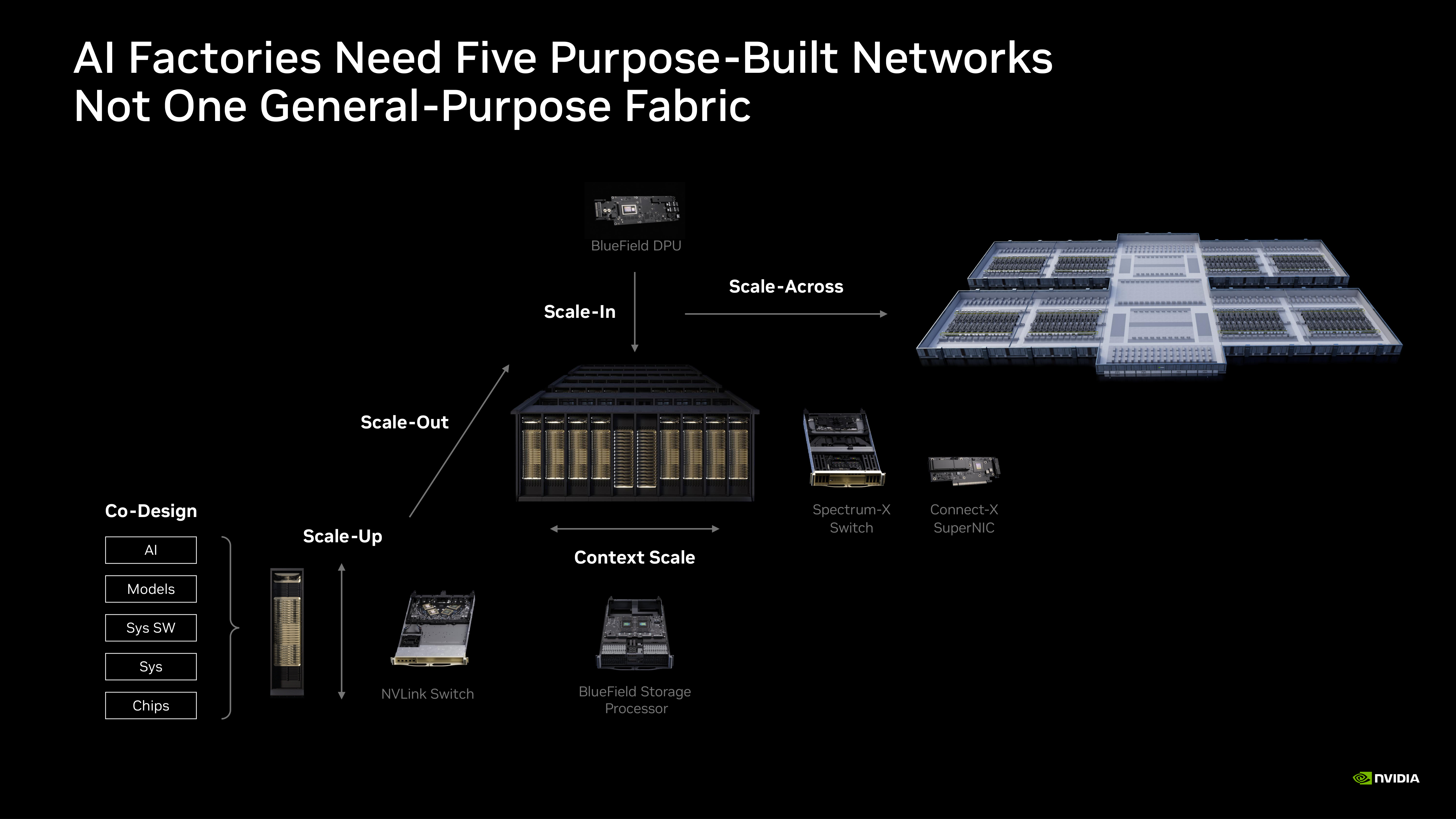
The five network roles distinguish:
- a) tightly coupled accelerators,
- b) wider jobs,
- c) infrastructure services,
- d) reusable context,
- e) and remote sites.
Their traffic travels different distances and tolerates different delays.
Spectrum-X combines NICs, switches and deployment software to reduce lost accelerator time from congestion and faults. The relevant delay includes queueing, completion handling and recovery as well as transmission time.
1) Reduce interference between competing jobs
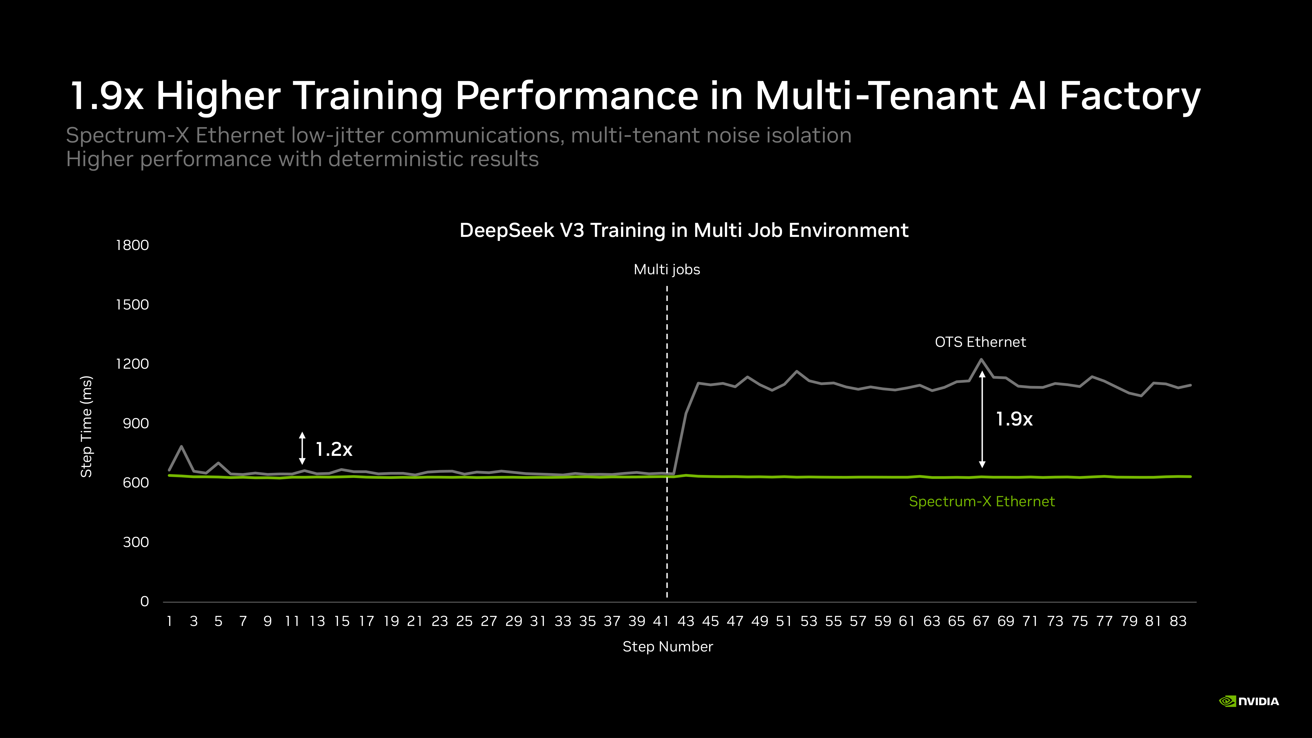
- Step number runs horizontally and training-step time in milliseconds vertically.
- After the dashed multi-job marker, the gray reference rises toward roughly 1,100 ms while the green Spectrum-X trace stays near its earlier level.
- Spectrum-X coordinates three actions:
- Switches select less congested paths using link conditions.
- NICs place packets correctly even when those paths change arrival order.
- Telemetry informs sending-rate control, limiting new traffic when paths are already busy.
- Adding traffic to a congested path would otherwise lengthen its queue instead of increasing useful delivery.
- A distributed dependency occurs when a GPU needs data or a combined result from other GPUs before its next operation can proceed.
- Network contention can delay that result after local arithmetic has already finished, leaving the GPU waiting.
- Reducing that wait shortens the training step and gives the accelerator more time for useful work, even though its arithmetic units are unchanged.
2) Distribute traffic across network planes
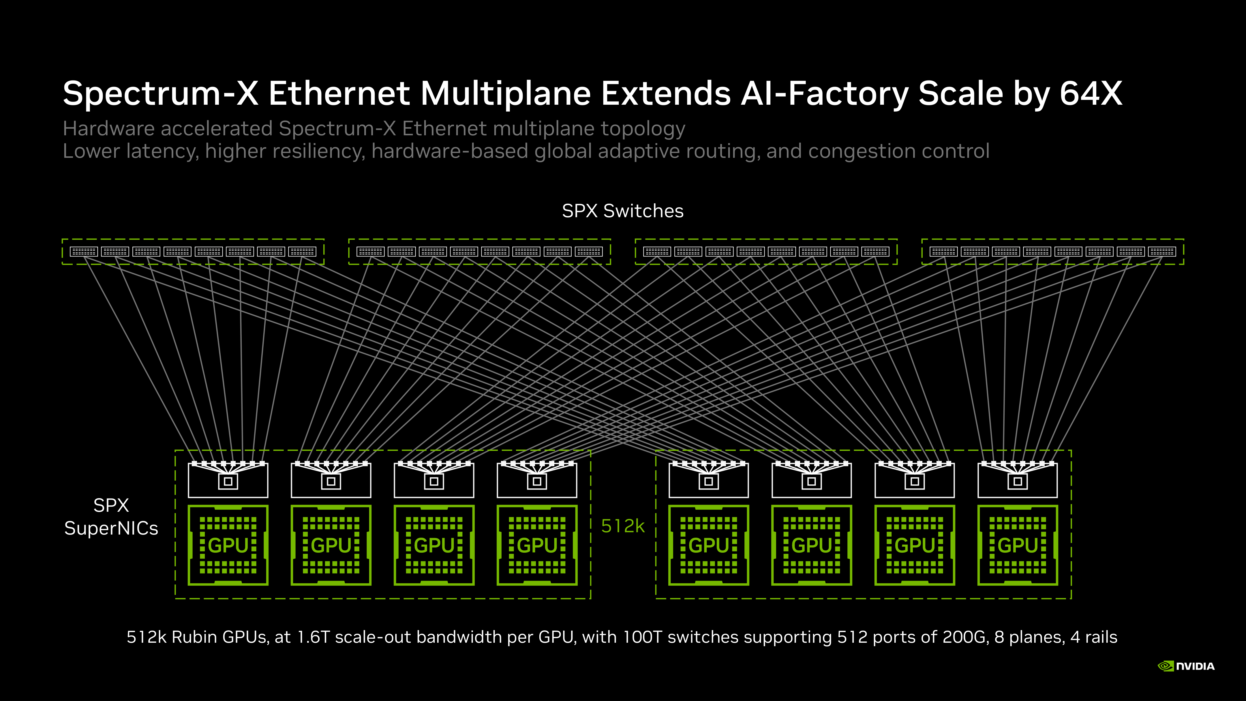
- A plane is a separate network path through a switch group. The multiple lines from each SuperNIC show an endpoint distributing its traffic across those paths.
- A GPU's 1.6 Tb/s connection is divided into eight 200G planes. The drawing does not assign the entire 1.6 Tb/s to every line.
- This gives traffic more than one route and leaves surviving paths available after a failure, although redistributing traffic can increase their load.
3) Preserve useful progress during recovery
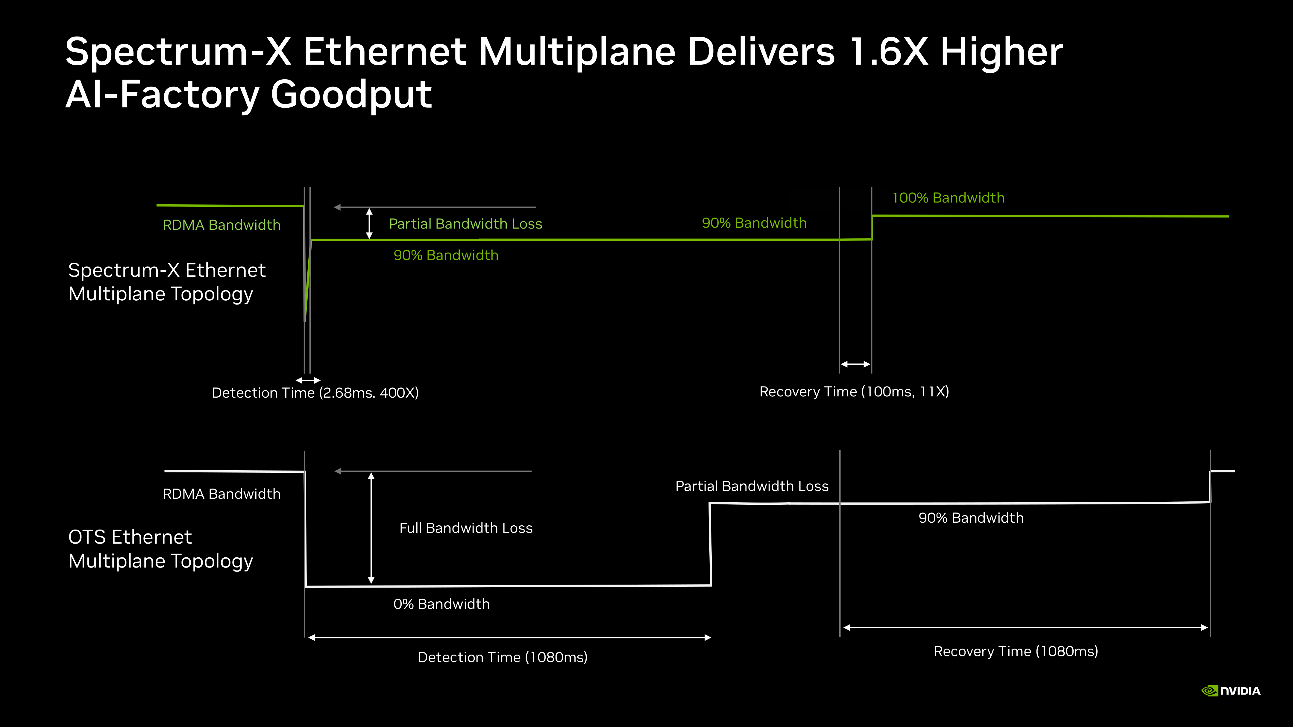
- Read time from left to right.
- The upper trace retains about 90% of bandwidth during the illustrated disruption, while the lower reference includes an interval with no bandwidth.
- Surviving planes continue carrying traffic while recovery proceeds, preserving most of the connection capacity.
- Application throughput also depends on redistribution, surviving-path congestion, and how long recovery takes.
- Goodput measures useful application work completed over an interval that includes interruptions and recovery.
- A healthy-link bandwidth measurement omits the time a job spends stalled or repeating work after a disruption.
- Keeping the job communicating over surviving paths during a failure can increase completed work over that interval, even if peak port speed is unchanged.
4) Change the optical connection as the network grows
The move from front-panel optical modules toward the switch was covered in On CPO, Part 1. Spectrum-X provides a concrete example of that shorter electrical path and the assembly it requires.
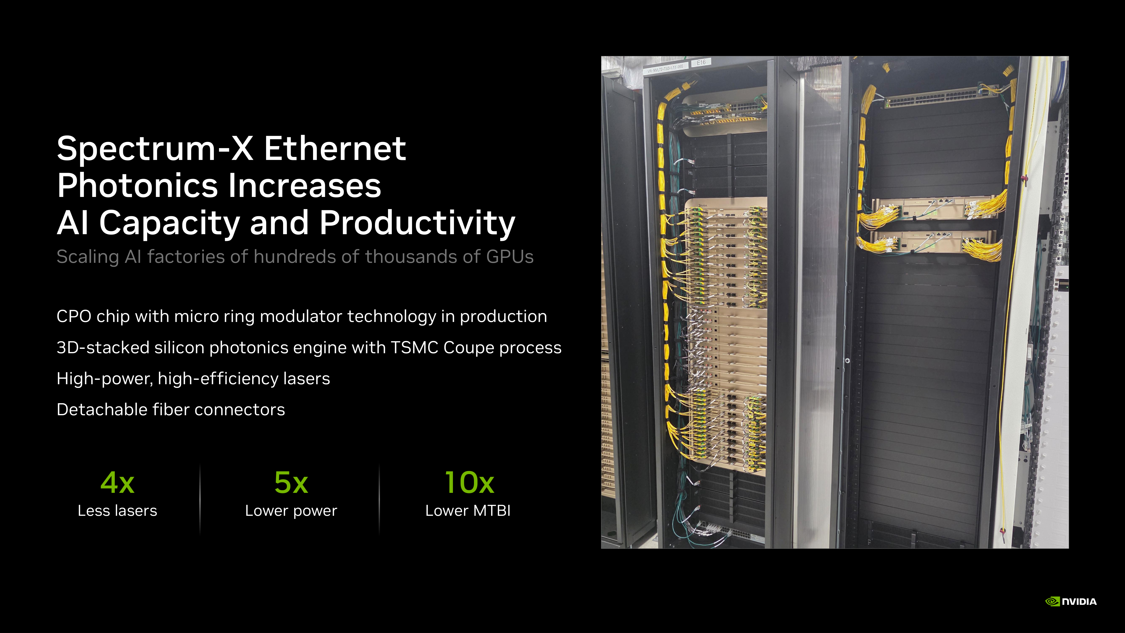
- Co-packaged optics moves electrical-to-optical conversion close to the switch silicon.
- The electrical signal travels a shorter route before becoming light, reducing the burden of driving it to a separate module.
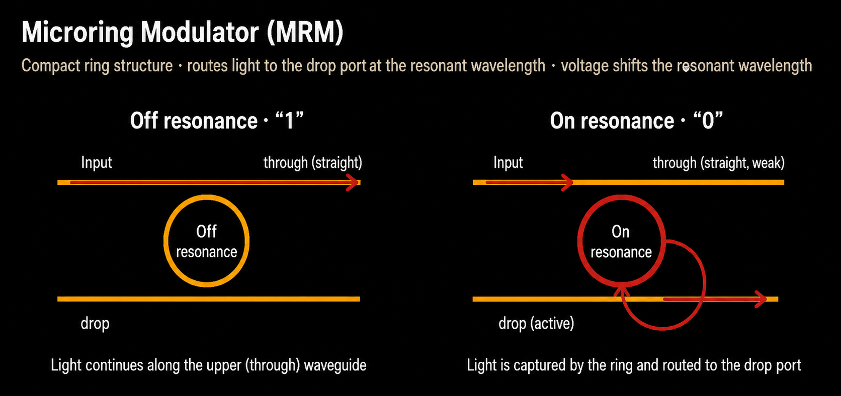
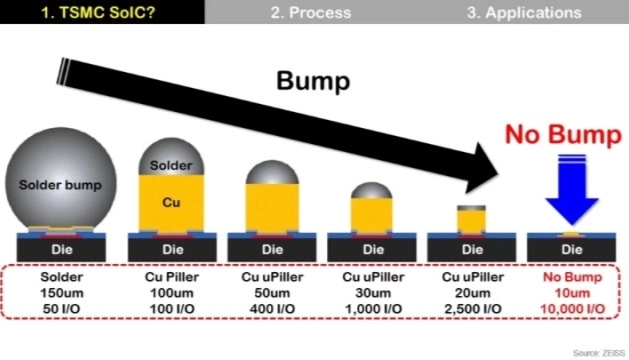
- The disclosed engine uses micro-ring modulators to encode data onto the light. COUPE technology from TSMC (NYSE: TSM) stacks its photonic and electronic circuits closely together.
- Detachable fibers let the external optical connection be connected and serviced without permanently attaching the cable to the assembly.
- This addresses link power and physical connections. Routing and congestion control still determine how well traffic uses those links.
- The disclosed manufacturing chain assigns distinct roles:
- TSMC packages the photonic and electronic ICs.
- SPIL, part of ASE Technology Holding (NYSE: ASX), appears as the testing partner in the assembly flow.
- Lumentum (NASDAQ: LITE) provides the laser sources.
- Foxconn (Hon Hai, TWSE: 2317) assembles the complete switches.
- A switch deployment creates demand across optical engines, lasers, testing and system assembly.
- The suppliers describe different deployment stages:
- In August 2026, Foxconn targeted CPO-switch mass-production shipments in Q3 2026.
- In August 2026, Lumentum said scale-out CPO laser shipments were already under way. It expected high-volume scale-up laser shipments in the second half of 2027 for customer deployments in 2028.
- The latter timing is Lumentum’s broader customer outlook; it does not identify a specific NVIDIA scale-up design win.
5) Extend the system across sites and to other accelerators
Scale-across: Account for distance between sites
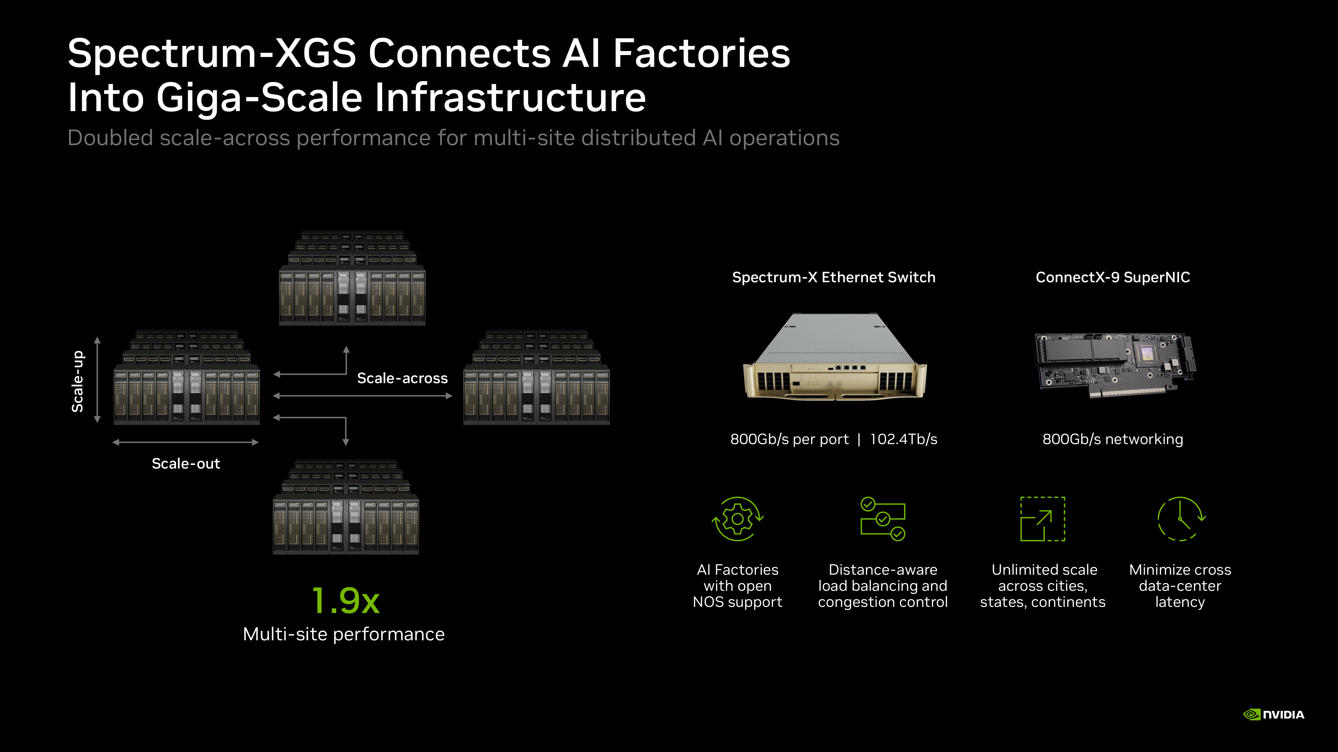
- The arrows between installations represent a longer communication scope than the links inside one rack. Spectrum-XGS adds distance-aware load balancing and congestion control for that scope.
- Feedback from a remote site returns later, so sending decisions must accommodate more data in flight and slower knowledge of congestion.
- These controls can reduce avoidable waiting, but they cannot remove the signal's travel time between sites. The reported 1.9× result belongs to the disclosed multi-site comparison.
Attach custom XPUs to the scale-up platform
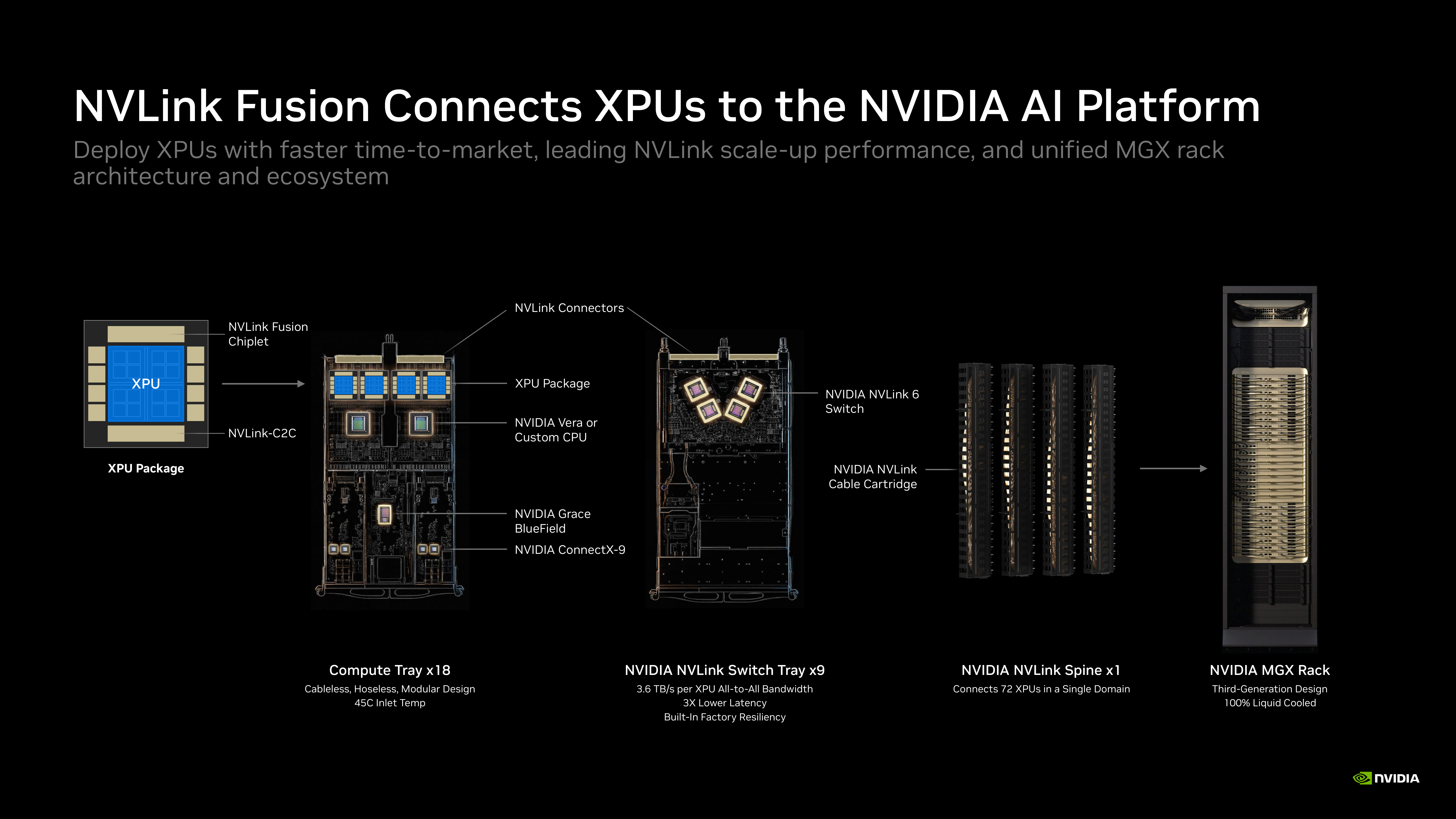
- The custom XPU connects through NVLink-C2C to the Fusion chiplet, then to NVLink switches and the rack. The chiplet supplies the bridge into NVIDIA's tightly coupled scale-up system.
- This could let NVIDIA supply the interconnect and rack even where a customer designs its own accelerator. Adoption still requires the custom package and software to support that connection.
Announced adoption cases
- AWS Trainium4: On December 2, 2025, AWS and NVIDIA announced that Trainium4 is being designed to integrate with NVLink 6 and NVIDIA's MGX rack architecture through NVLink Fusion. This is an announced integration rather than an already deployed Trainium4 system: Amazon expects Trainium4 deliveries to begin in 2027.
- d-Matrix Raptor XPU: On September 10, 2026, d-Matrix announced plans to connect its next-generation Raptor XPUs through NVLink Fusion, using NVIDIA's NVLink scale-up network, Spectrum-X scale-out network and MGX rack architecture. This is an announced integration, not evidence of an already deployed Raptor system.
4. SRAM and dataflow designs take different routes to low latency
(1) NVIDIA LPU: plan execution and communication together
The LPU combines:
- a) fast distributed SRAM,
- b) and a compiler-planned execution schedule.
NVIDIA’s Groq 3 LPX system brings the Groq LPU architecture alongside GPUs. Different work splits retain GPU capacity and throughput while accelerating the stages most sensitive to response time.
1) Schedule operations and operand arrival together
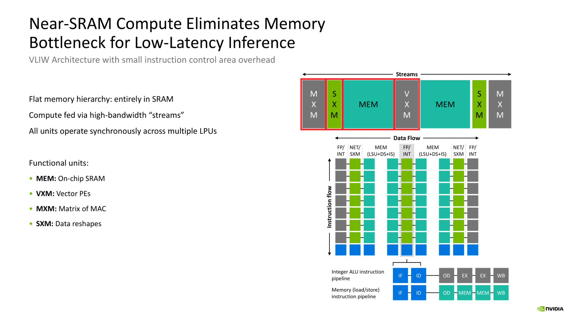
- The four red boxes identify one of each resource type along the horizontal stream. From left to right:
- MXM performs matrix arithmetic.
- SXM rearranges data for the next operation.
- MEM stores data in SRAM.
- VXM performs vector operations.
- The vertical instruction paths control when each resource acts.
- The compiler schedules operations and operand arrivals together, including routes across chips.
Plan data movement as part of execution
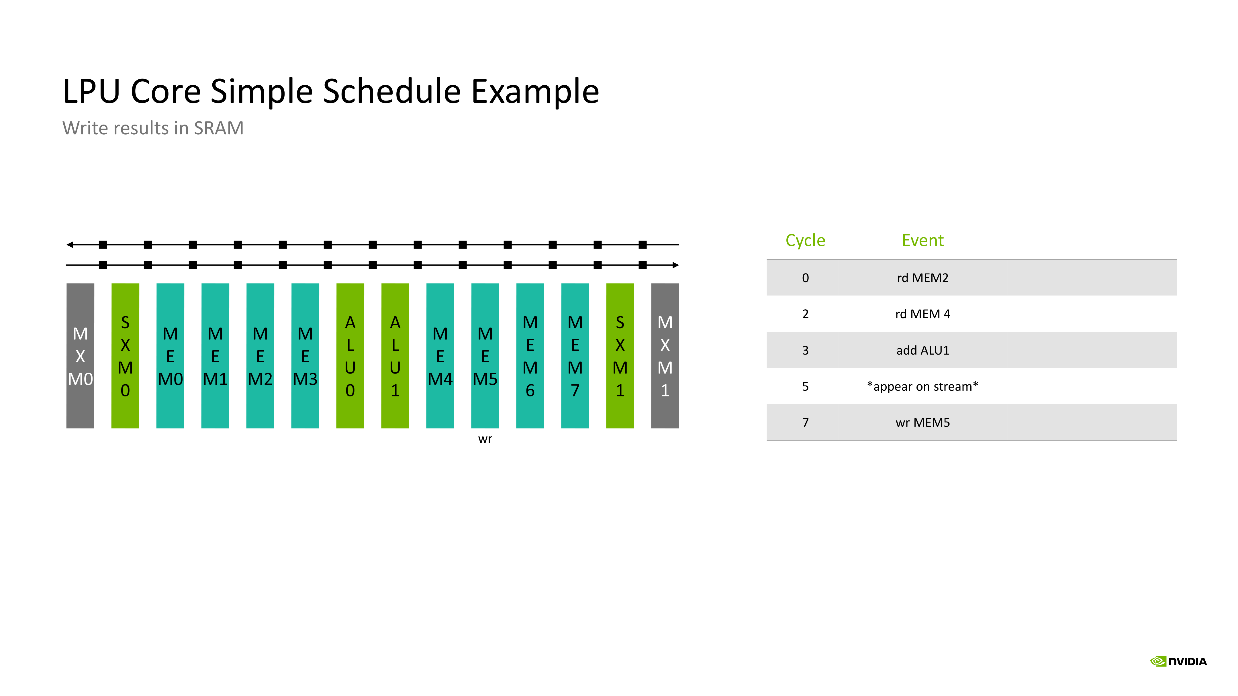
- The table schedules both input reads, the addition, and the result write as one sequence. Different input travel times are handled in advance so both values reach arithmetic when needed.
- Planning those movements can reduce runtime coordination and make execution predictable. The compiler must construct a valid schedule for the model and the available hardware.
Bridge variable arrivals into the planned domain
- Requests and their input data arrive at variable times. The planned LPU schedule can begin only after the inputs needed for that invocation are ready.
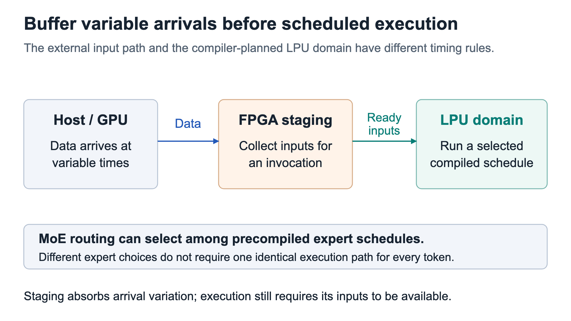
- The host / GPU side supplies data at variable times.
- FPGA staging collects the input for an invocation, after which the selected compiled schedule can run.
- For mixture-of-experts work, hardware can choose among precompiled schedules according to the selected expert.
- Deterministic execution does not require every token to use the same expert or path.
Use the schedule to anticipate electrical demand
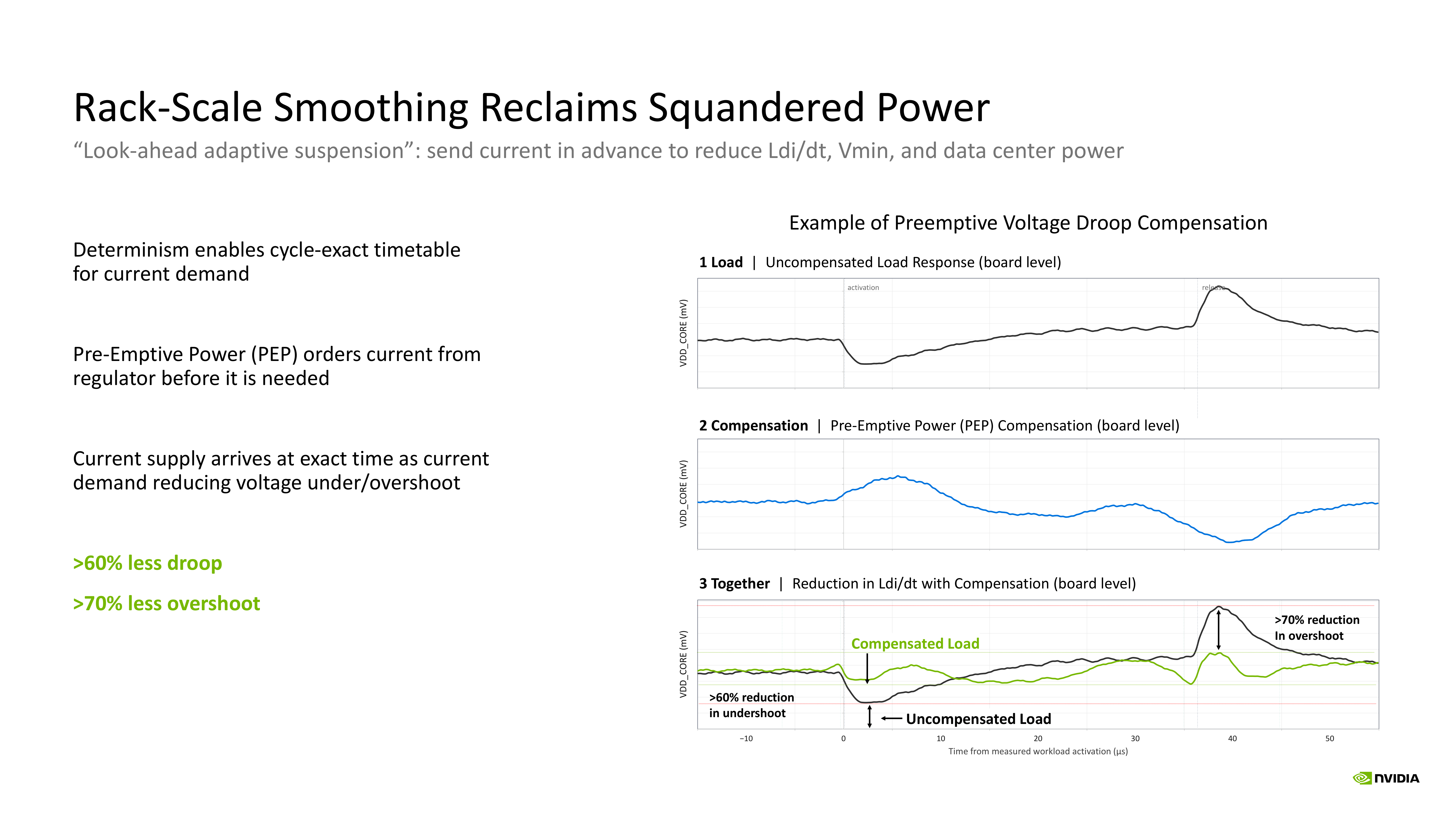
- Time from activation runs horizontally in microseconds; core voltage runs vertically in millivolts.
- The top black trace dips when work suddenly draws current, then overshoots when that demand ends.
- The planned execution schedule reveals those changes in advance.
- The middle blue trace shows the regulator preparing current before the change arrives.
- The lower green trace shows smaller voltage excursions after that compensation.
- The reported reductions of over 60% in undershoot and over 70% in overshoot measure voltage stability.
2) Account for the cost of distributed SRAM capacity
- Each LPU has limited on-chip SRAM capacity. A large workload may need the combined memory of many LPUs.
- That memory is distributed across chips and racks. Reaching it requires communication, so access time includes network delays as well as local SRAM access.
- Assembling enough capacity therefore adds devices, connections and power consumption.
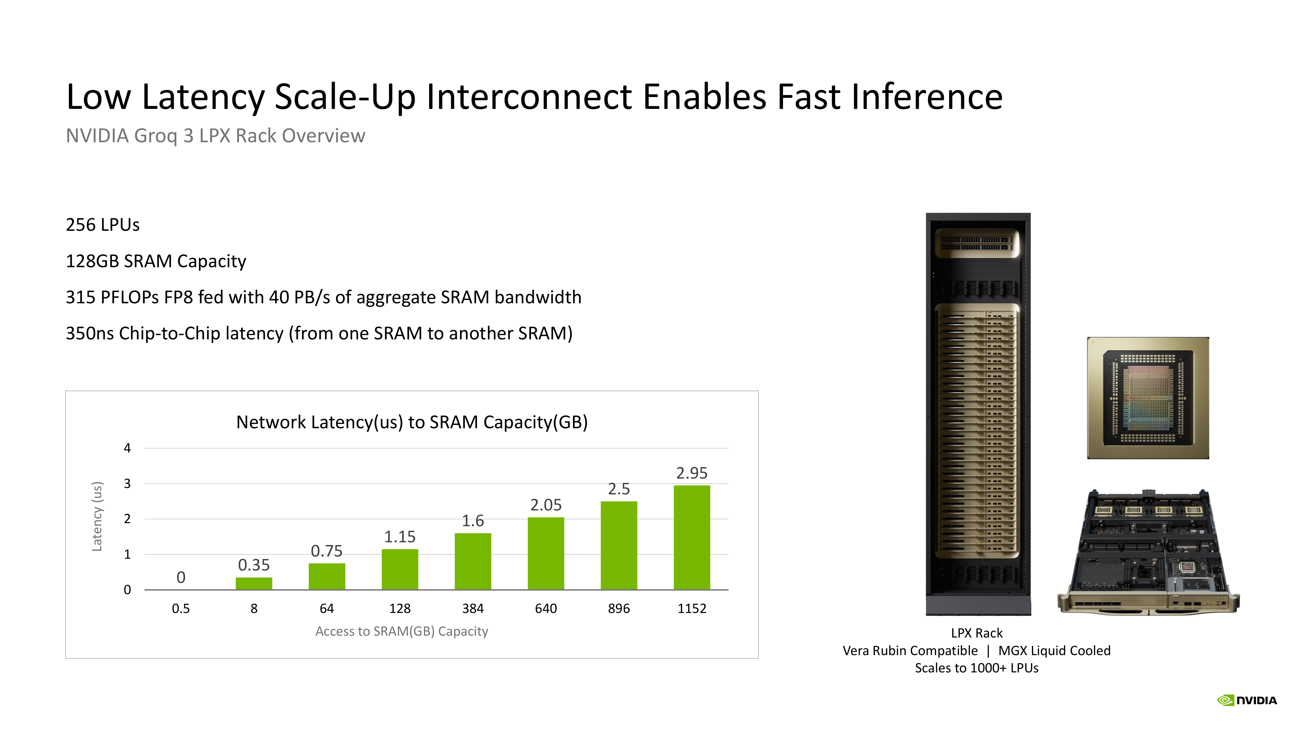
- The lower chart plots reachable SRAM capacity in gigabytes horizontally and network latency in microseconds vertically.
- The first 0.5 GB point has zero added network latency. This does not mean the SRAM itself takes no time to access.
- Reaching the rack's combined 128 GB of SRAM is labeled 1.15 μs. That capacity is spread across 256 LPUs, and reaching larger multi-rack capacity adds more network delay.
- LPU performance depends on how much distributed hardware and communication a workload needs, as well as how quickly each chip accesses its own SRAM.
3) Choose what crosses the GPU / LPU boundary
The three choices divide inference work and KV-cache ownership between the GPU and LPU. That division determines what data must move between them.
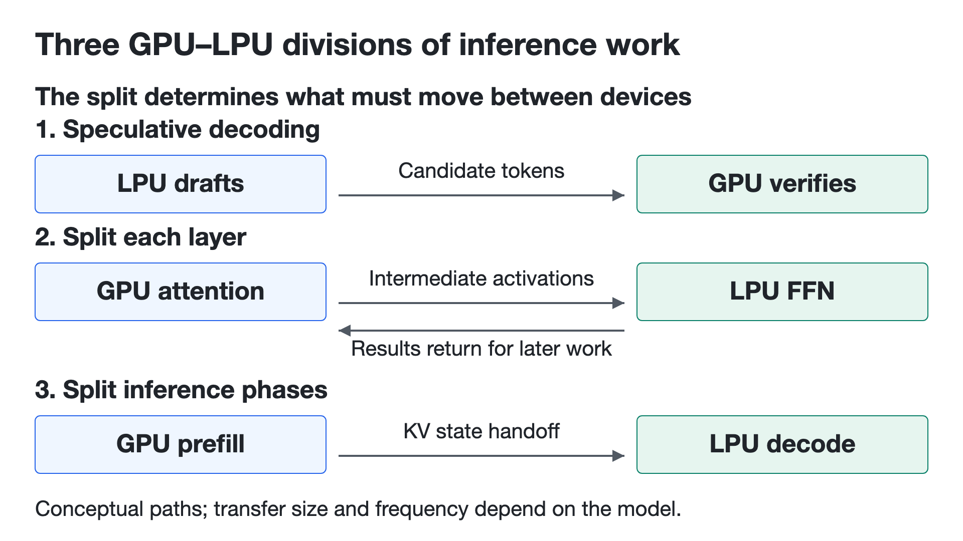
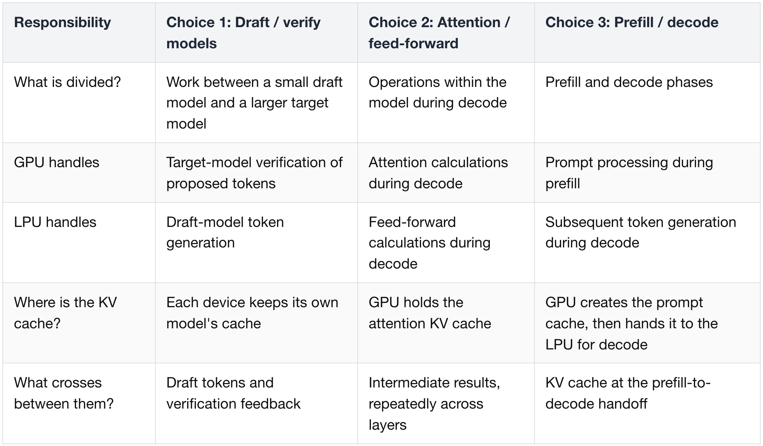
- Only Choice 3 explicitly assigns prefill to the GPU and decode to the LPU.
- Choices 1 and 2 describe how generation work is divided; their diagrams do not separately assign prefill.
Choice 1: Draft on the LPU, verify on the GPU
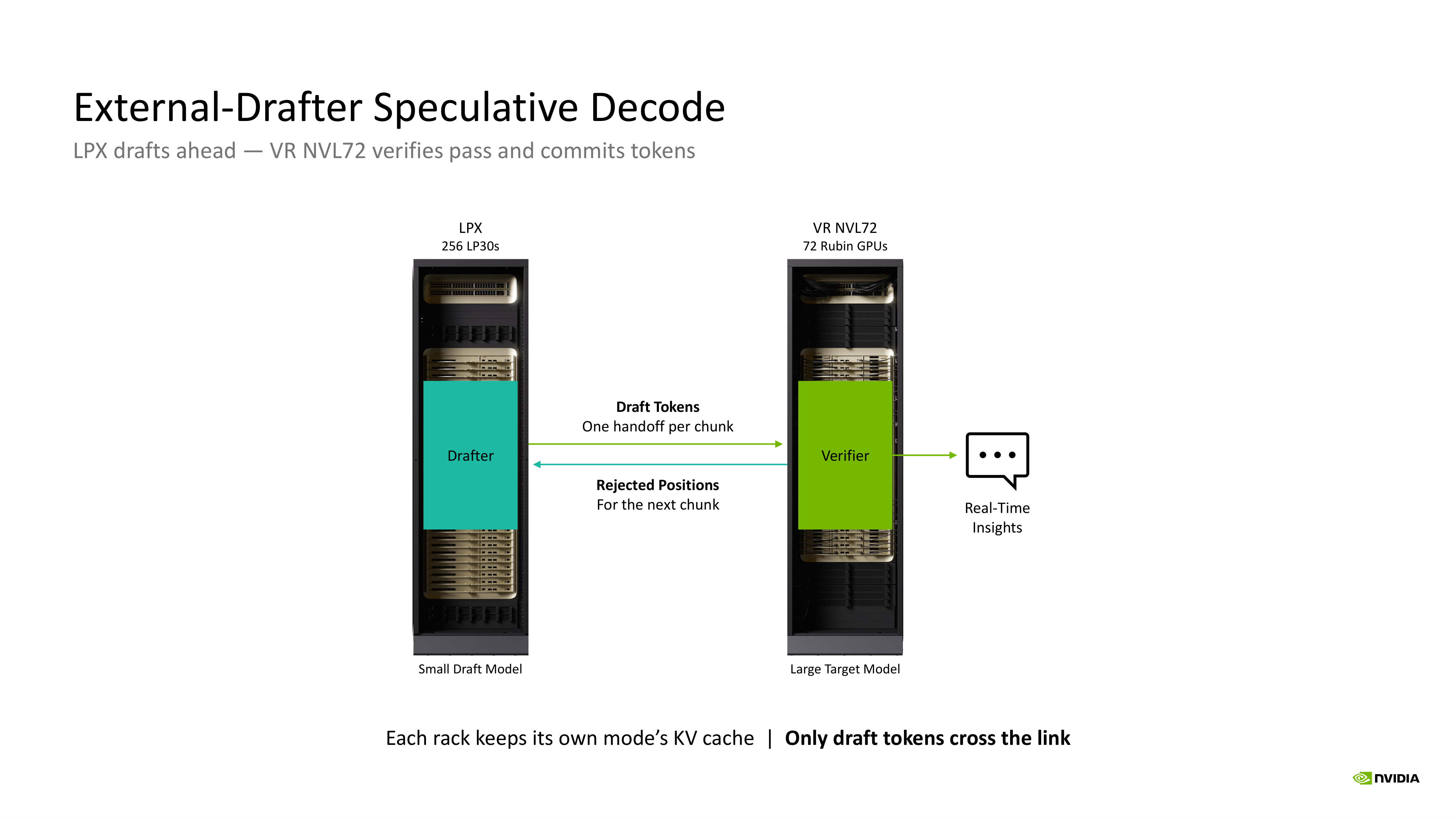
- A small draft model on the LPU proposes a group of next tokens and sends them to the GPU.
- The larger target model on the GPU checks those candidates together and accepts the valid continuation. Rejection information returns to guide the next draft.
- Each model keeps its own KV cache, so this split sends token proposals and feedback rather than transferring the cache between models.
- Accepting several draft tokens lets one verification pass advance several output positions. Rejected candidates still cost drafting and checking time, so the gain depends on acceptance and the time spent on both devices.
Choice 2: Keep attention on the GPU and feed-forward work on the LPU
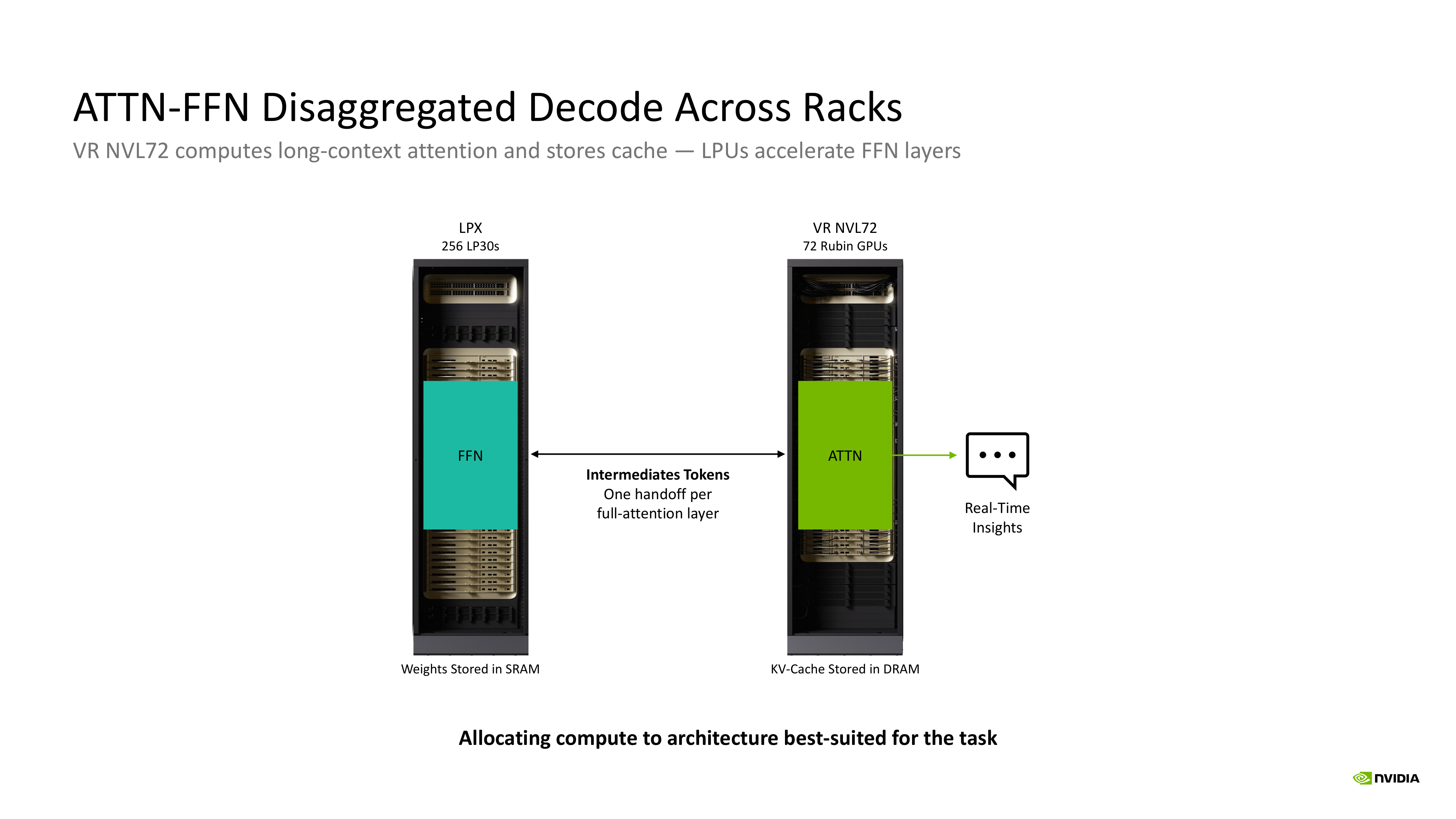
- The GPU computes attention using the KV cache in its DRAM and sends the resulting activations, or intermediate values, to the LPU.
- The LPU applies the feed-forward layers using weights held in SRAM, then returns results needed by the GPU's next attention stage.
- This exchange repeats as the model advances through its layers. Faster LPU computation must save more time than these repeated transfers and waits add.
Choice 3: Process the prompt on the GPU, then decode on the LPU
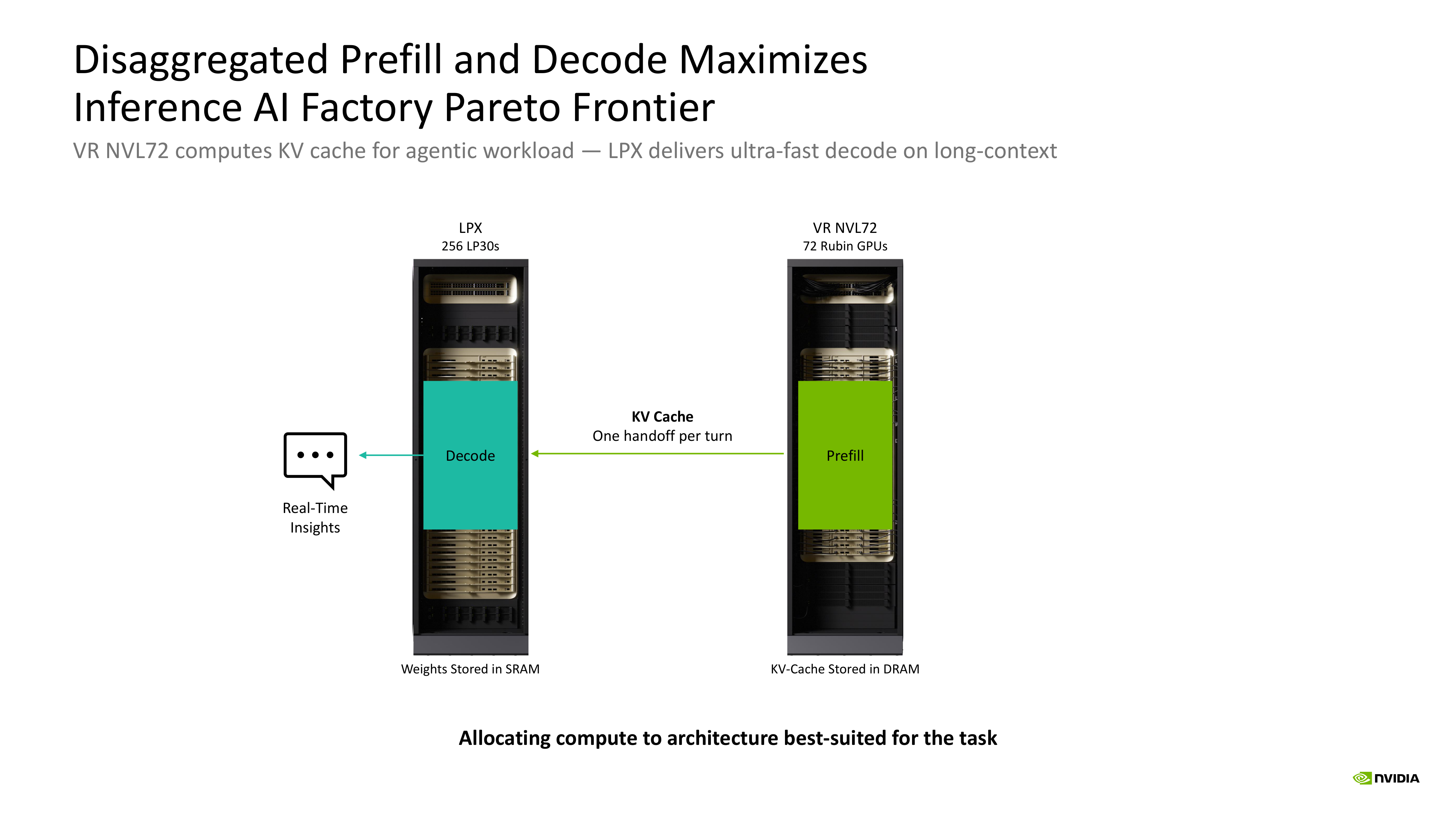
- The GPU processes the prompt in the prefill phase and creates the KV cache needed to attend to that prompt.
- The GPU transfers that cache when it hands the request to the LPU. This handoff is the prefill-to-decode phase boundary.
- The LPU then runs decode itself, generating successive output tokens. Unlike Choice 2, it does not repeatedly exchange intermediate results with the GPU at every layer.
- The LPU must receive the KV data needed for its next calculation. If that data has not arrived when the calculation is ready to start, the LPU waits, delaying the first output token.
When can computation overlap the KV transfer?
- Overlap means doing useful computation while the KV data is being copied. The overlapping calculation must not need the data that is still arriving.
- As a hypothetical example, assume the transfer takes 10 μs. If the LPU has no independent work ready for this request, it waits the full 10 μs for the data.
- If the LPU can instead spend the first 6 μs completing independent calculations for the same request, the transfer continues during those calculations. When they finish, 4 μs of copying remains, so the next KV-dependent calculation waits another 4 μs.
4) Compare efficiency at a chosen response speed
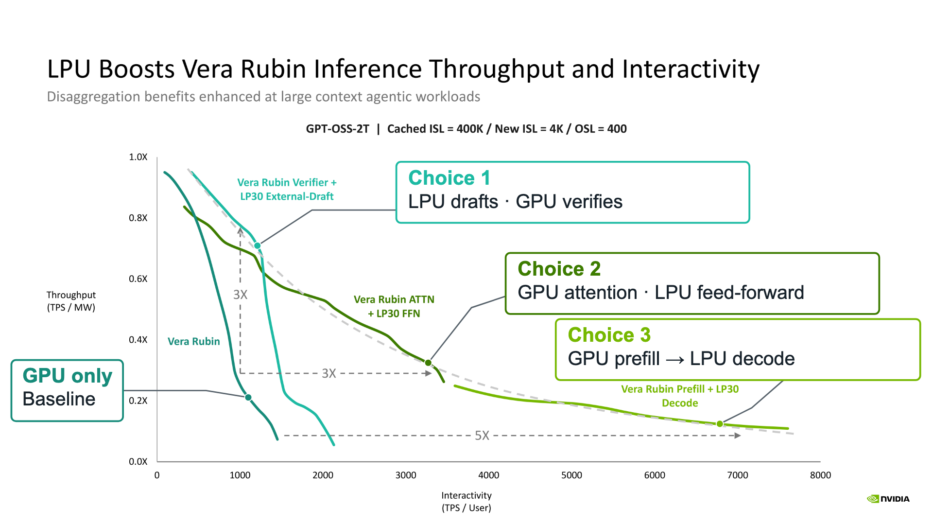
- The horizontal axis shows tokens per second received by one user. Farther right means faster output for that user.
- The vertical axis shows total tokens per second across users, divided by power in megawatts and displayed relative to a 1.0× reference. Higher means more total output for the power used.
- Dark teal is the GPU-only Vera Rubin system. Turquoise adds LPU drafting, dark green puts feed-forward work on the LPU, and light green puts decode on the LPU.
- NVIDIA’s comparison uses GPT-OSS-2T with 400K cached input tokens, 4K new input tokens and 400 output tokens. The relative gains apply to that long-context setup.
5) Bring LPUs into CUDA
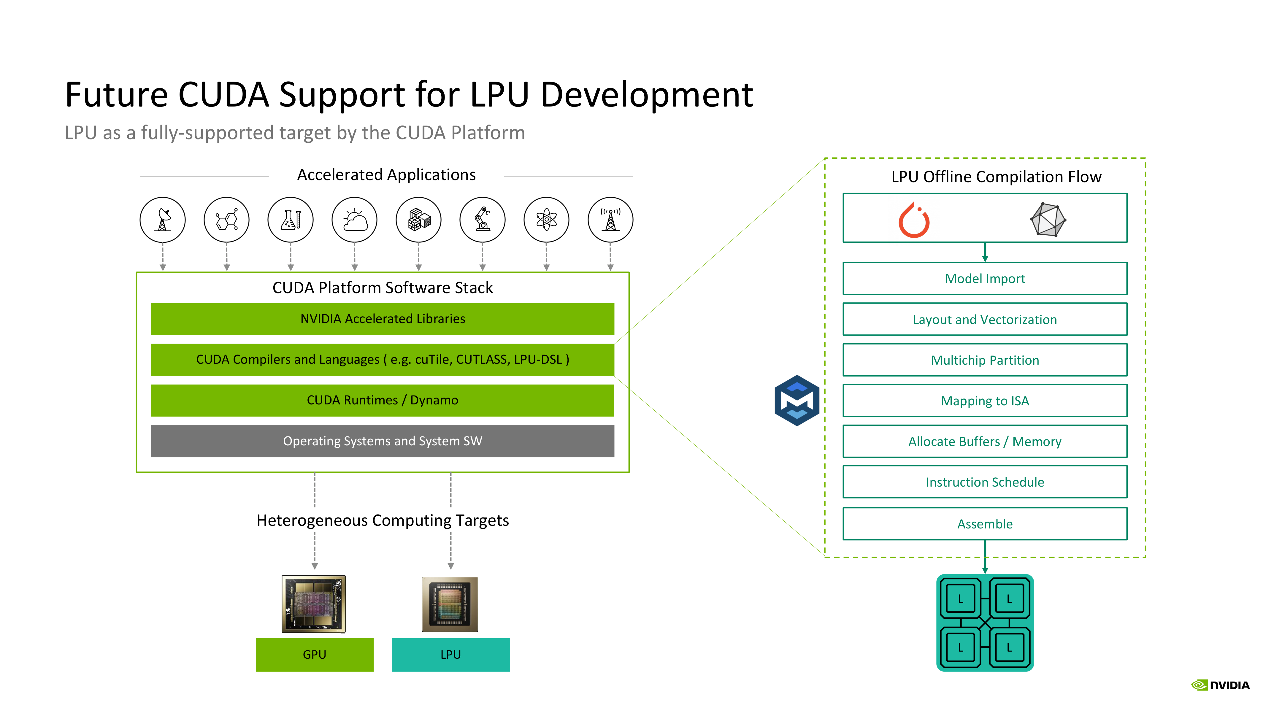
- NVIDIA plans to let applications use GPUs and LPUs through the same CUDA platform, reducing software changes.
- The LPU compiler still has to divide the model, assign operations and memory, and schedule computation and data transfers.
- CUDA support is a future capability in this presentation. Hardware production does not mean that support is ready.
- In August 2026, NVIDIA said Groq 3 LPX was in full production. Volume shipments were planned later that quarter, starting with Nebius (NASDAQ: NBIS).
- NVIDIA also noted that faster output per user can reduce total throughput and raise cost per token.
(2) Cerebras CS-4: keep more communication on the wafer
1) Build a three-wafer system around the existing wafer design
- Cerebras (NASDAQ: CBRS) places compute and SRAM across a wafer so nearby operations can exchange data without leaving it.
- CS-4 combines three WSE-3 Turbo wafers and redesigns their power delivery, cooling and external connections.
- If a model spans those wafers, intermediate results must still cross the external links before dependent work on another wafer can start.
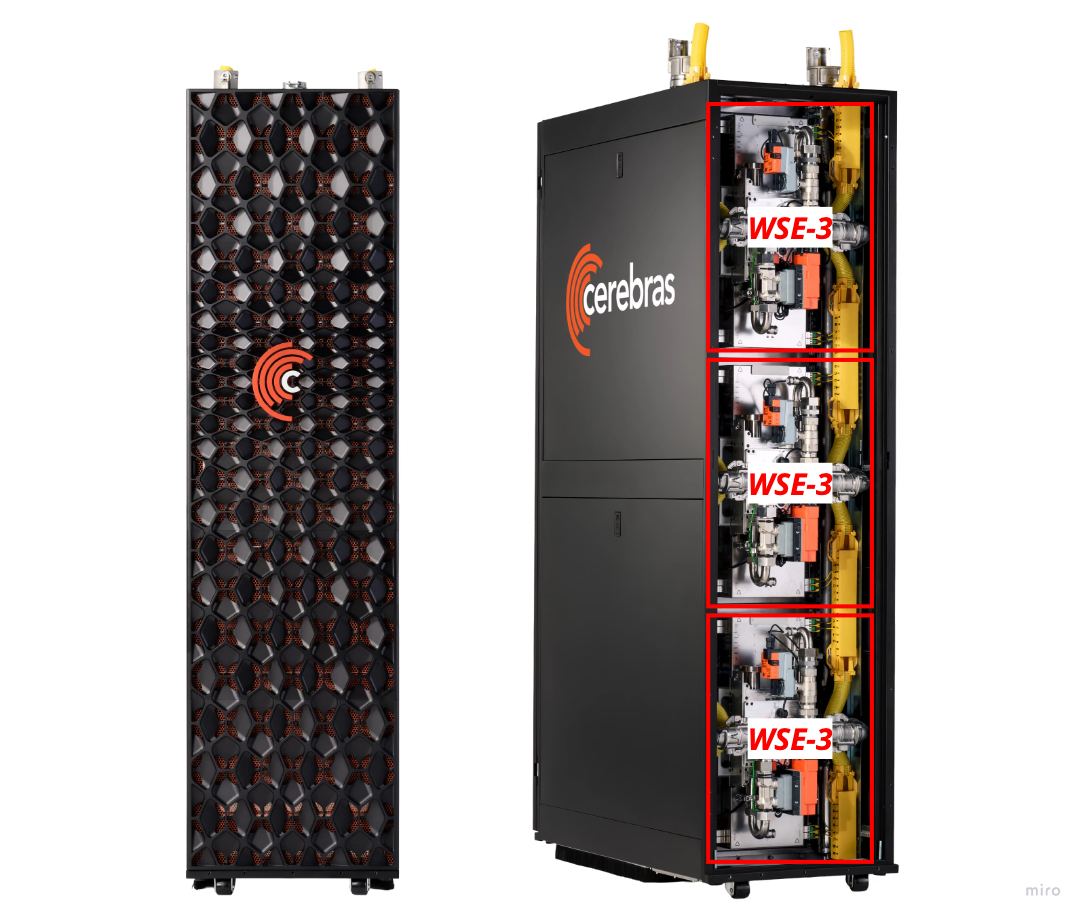
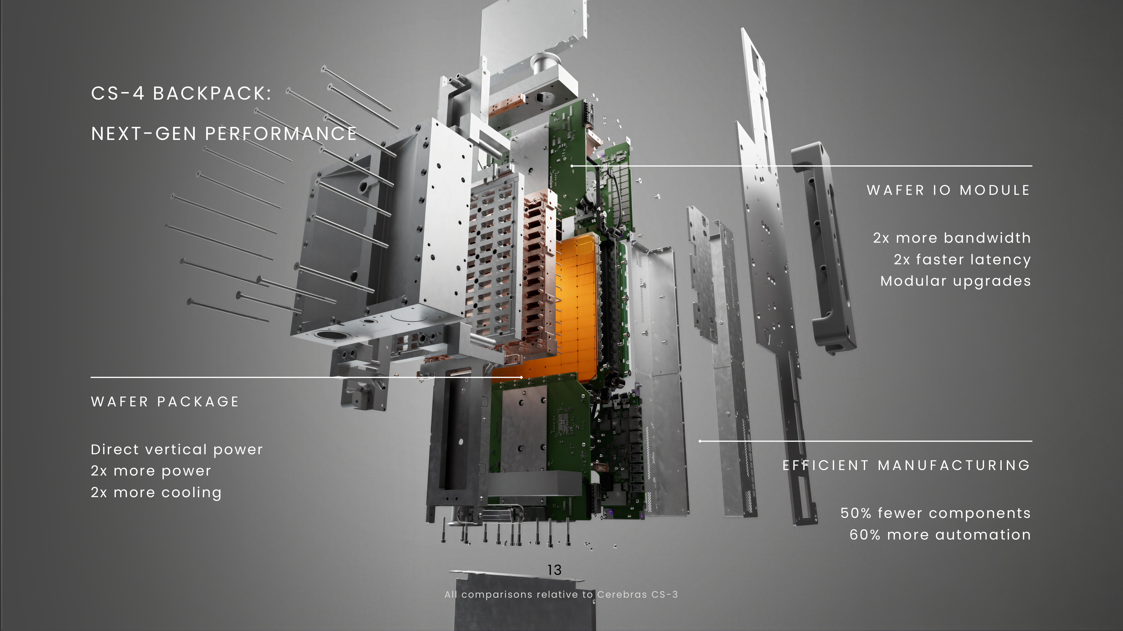
- The exploded assembly places the wafer package beside its power, cooling and replaceable I/O module. CS-4 installs three such assemblies. More power and cooling let the wafer run at a higher clock, while the I/O module carries data to and from other wafers or systems.
- In August 2026, Cerebras identified TSMC’s 5 nm process as its wafer supply. Management argued that this reduced exposure to more constrained leading-edge wafer capacity. Its current SRAM-based system also avoids HBM and CoWoS supply requirements, shifting more of the scaling work to wafer-system manufacturing, power and cooling.
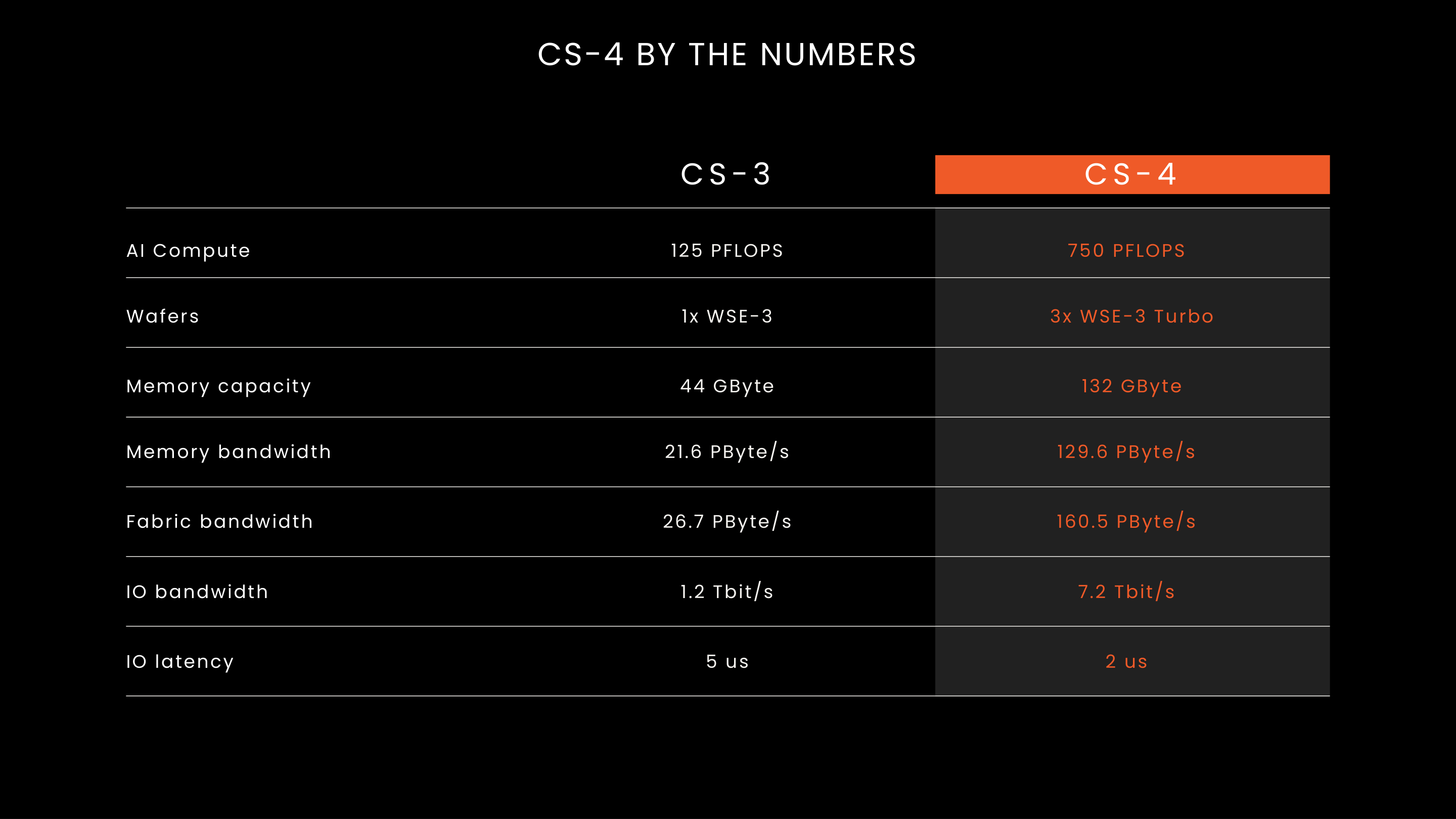
- Start with the wafer-count row: CS-4 combines three wafers, so the totals include more compute and SRAM hardware.
- The higher clock also increases the work that hardware can do each second. The comparison therefore combines more wafers with faster operation, supported by more power and cooling.
- Local memory bandwidth is reported in petabytes per second. External I/O is reported in terabits per second and carries data beyond a wafer.
- When one model partition sends a result to another wafer, it uses those external links. Unused local SRAM bandwidth cannot increase the speed of that transfer.
Separate faster access from additional storage
- SemiAnalysis’s CS-4 analysis compares the resources on one wafer. CS-4 reuses the WSE-3 silicon at a higher clock, so each wafer serves data faster while retaining the same number of SRAM bits.
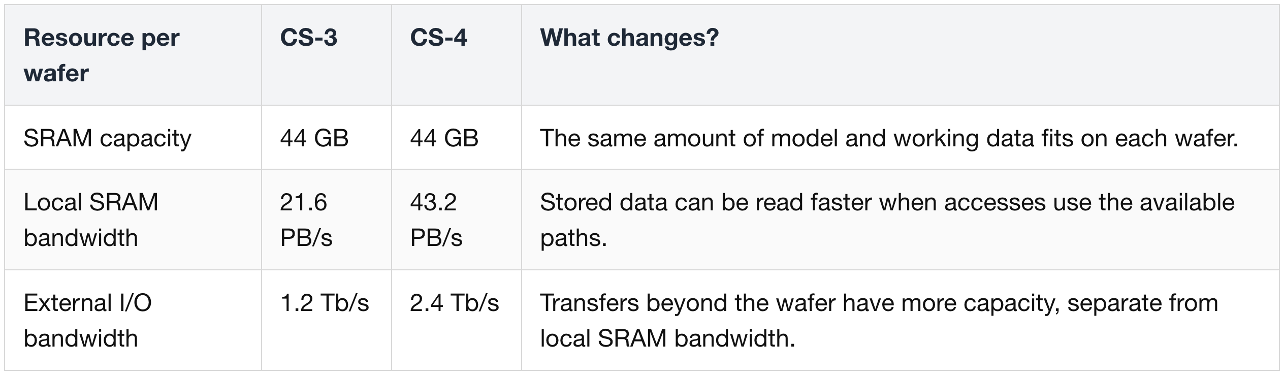
- Adding wafers increases storage as well as compute. Raising their clock increases the rate of work, but does not make a larger model or longer KV cache fit on one wafer.
- As a capacity illustration, 1.6 trillion weights at exactly four bits each occupy 800 GB before scales or other metadata. At the stated 44 GB per wafer, weights alone exceed eighteen wafers’ capacity. KV state, intermediate buffers and the actual model partition require additional room.
2) Shorten the high-current power path
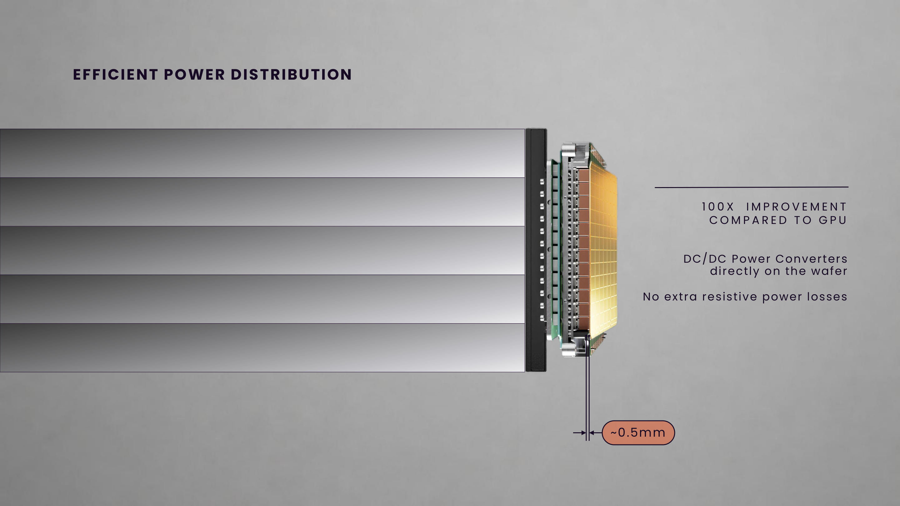
- The diagram puts power conversion close to the wafer.
- Power travels most of the route at higher voltage, which requires less current for the same power.
- Conversion near the wafer leaves only a short low-voltage, high-current path.
- The illustrated final path is roughly 0.5 mm, compared with 50 mm in the GPU arrangement.
- A shorter high-current path reduces resistive loss and unwanted heating.
3) Connect wafers without confusing local and external bandwidth
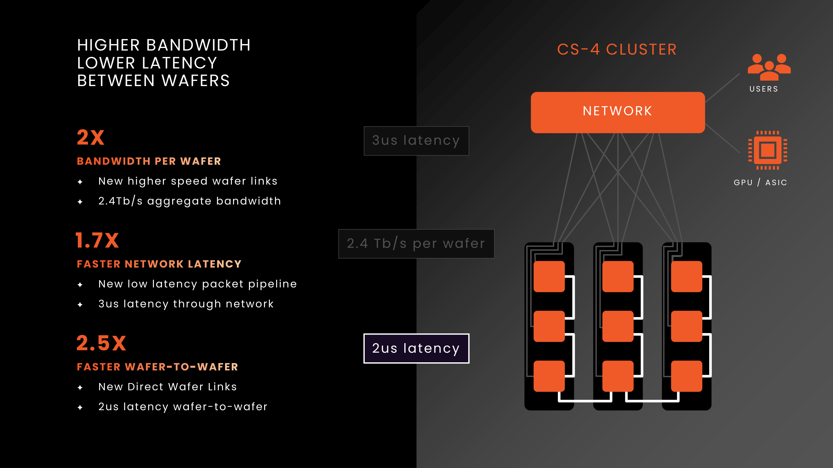
- The lower direct links connect wafers at a stated 2 μs latency.
- The upper network reaches users and other accelerators at a stated 3 μs latency.
- The 2.4 Tb/s per-wafer I/O rating applies to these external connections. It is separate from the much wider local SRAM fabric.
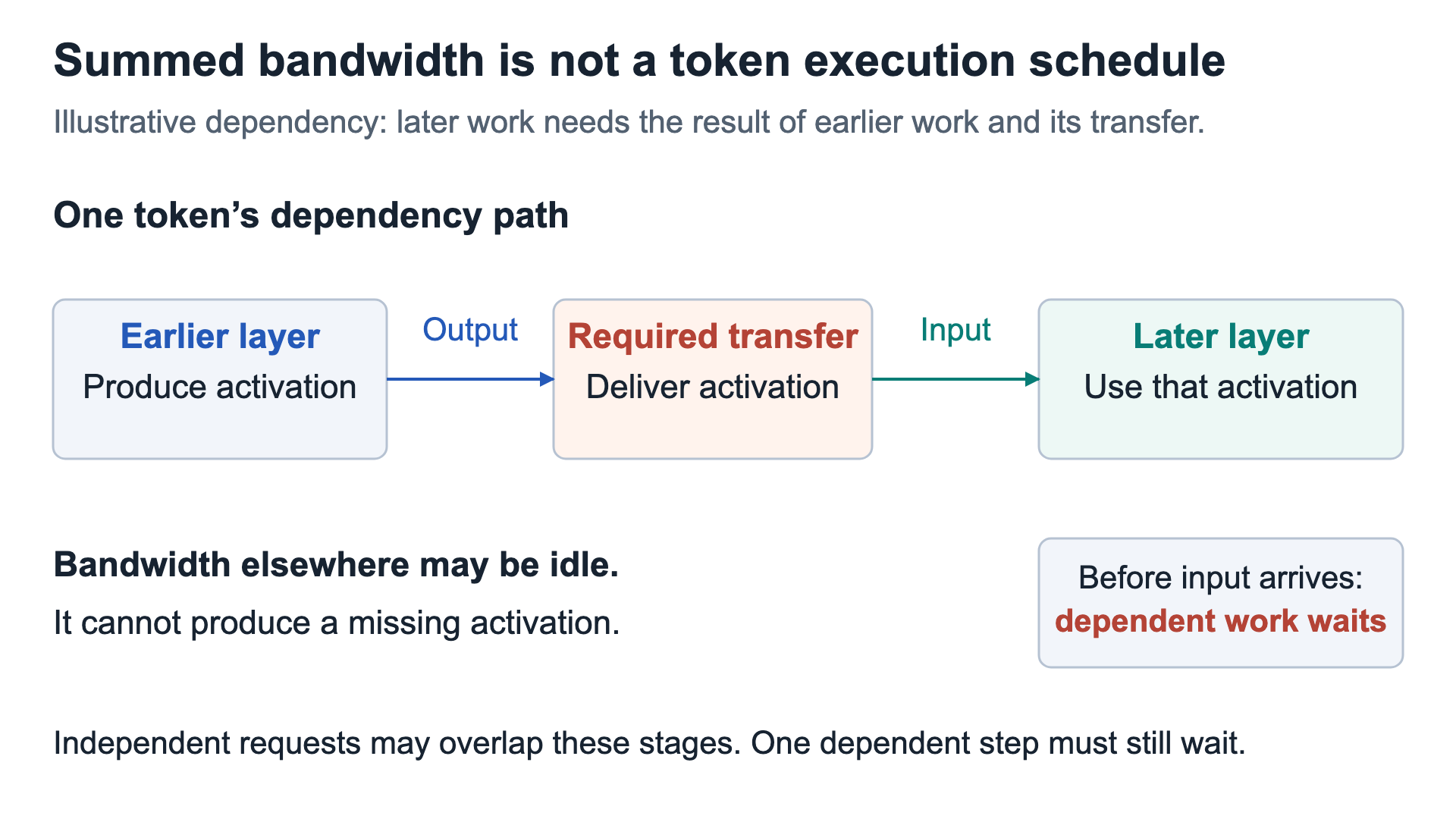
- Suppose the first part of a model runs on wafer A and the next part runs on wafer B. Wafer A must produce an activation and send it to B before B can perform the calculation that needs it.
- Other independent work can continue during the transfer. Any transfer time that cannot be hidden this way delays token generation, even if both wafers have spare local SRAM bandwidth.
- The replaceable I/O module uses programmable FPGA hardware to bridge wafer connections to Ethernet. This lets the external interface change without redesigning the wafer itself.
- Keeping an expert’s computation within one wafer can avoid splitting that expert across external links. A model spanning wafers still needs transfers between its assigned partitions.
- In August 2026, Cerebras described a planned combination with AMD Helios:
- Helios performs prefill, processing the incoming prompt.
- Cerebras systems perform decode, generating successive output tokens.
- KV state must move between them before dependent decode work can start.
Choose where to keep the KV cache and which work to assign to Cerebras
Combining Cerebras with an HBM accelerator creates a choice: a) transfer the KV cache for Cerebras to run decode, b) or keep attention and its KV cache on the HBM accelerator and repeatedly exchange intermediate results.
This matters because Cerebras has limited SRAM capacity to hold model weights and KV data.
The table compares what each processor does and what data must move over the connection between them.
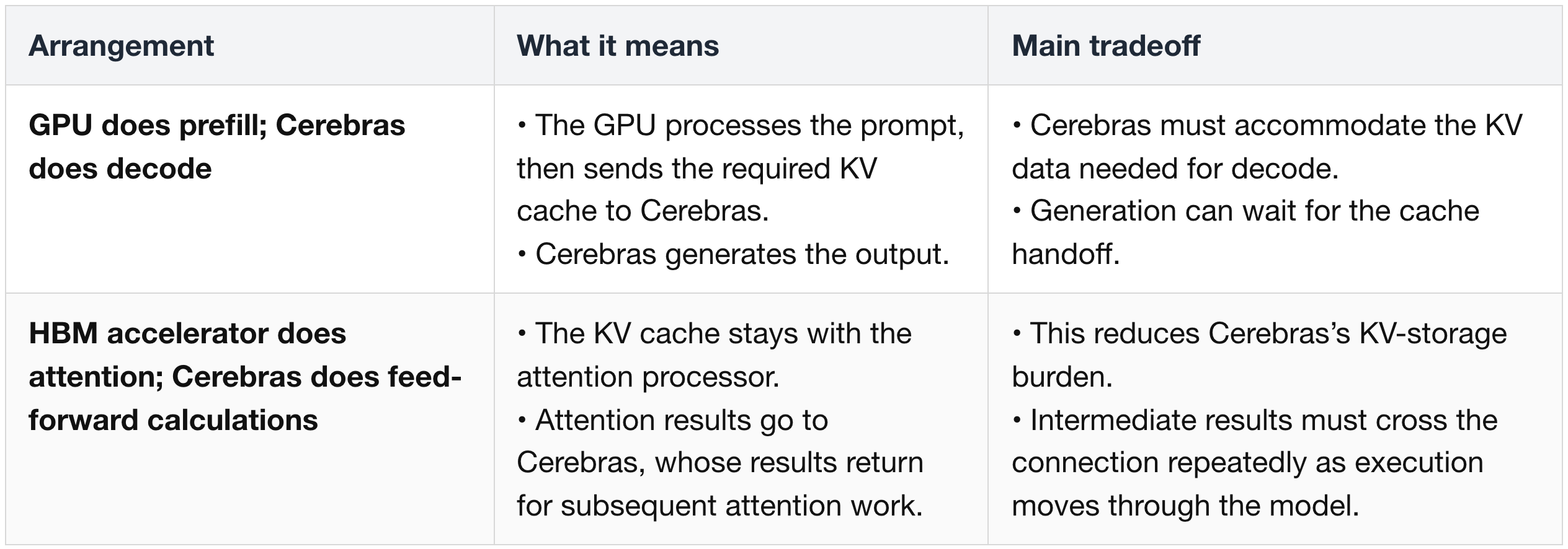
- The second arrangement is an architectural option discussed in the CS-4 analysis, distinct from the announced Helios prefill / decode split. It trades some SRAM storage demand for repeated communication.
4) Reuse the physical platform and separate capacity growth from compute growth
CS-4 establishes the physical platform

- The proposed Nexus rack would let CS-5 and CS-6 reuse the power delivery, cooling and modular I/O developed for CS-4. That would avoid redesigning the whole rack for each generation, provided the later hardware remains compatible.
CS-6 adds stacked DRAM beside wafer-scale SRAM
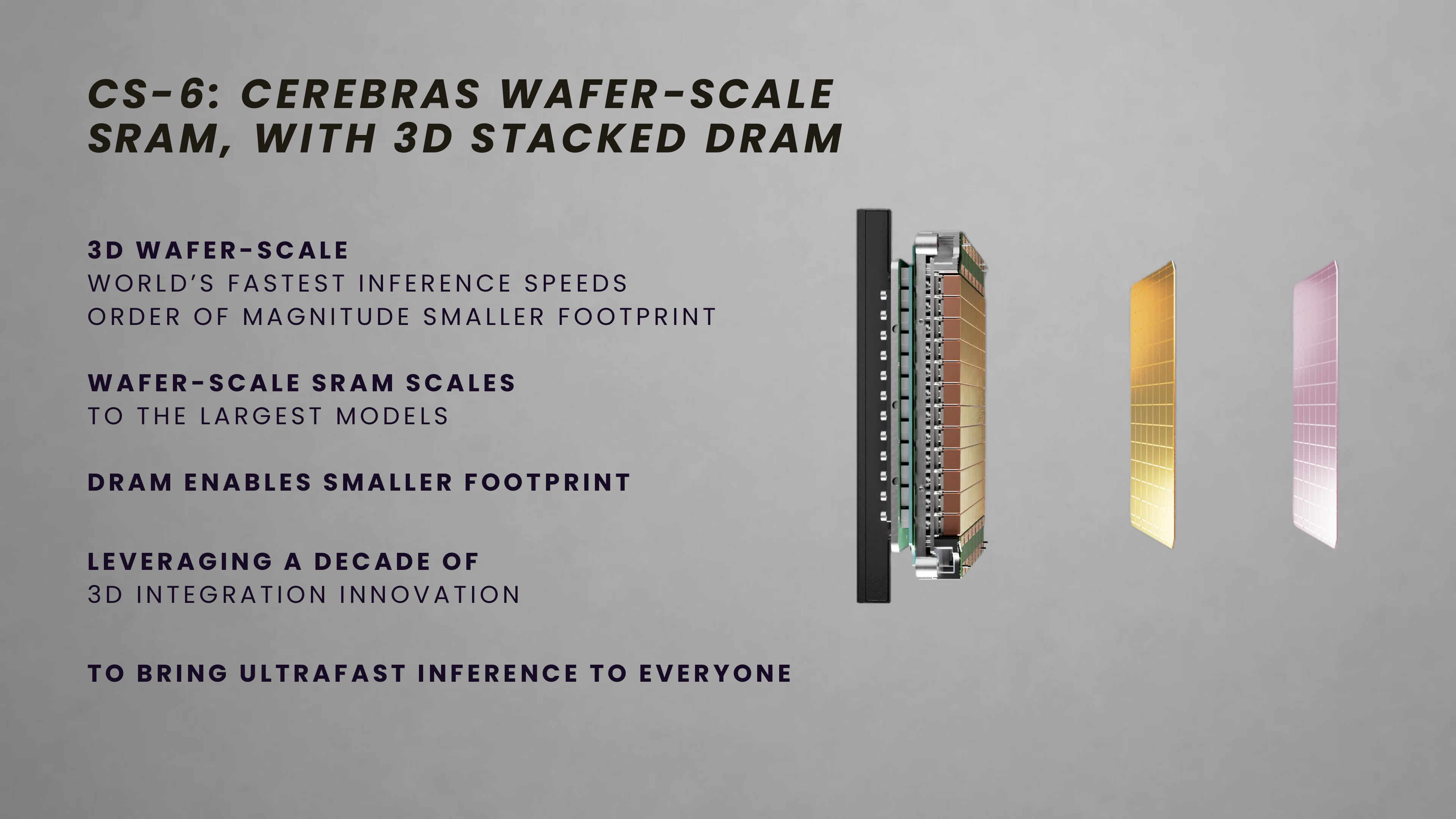
- Today, adding more wafer-scale SRAM capacity also adds the compute hardware on those wafers.
- The CS-6 concept adds a denser, 3D-stacked DRAM tier beside the SRAM. SRAM holds nearby working data, while DRAM provides additional storage.
- This would let the system add model capacity without adding a compute wafer for every increment of memory. The intended result is fewer compute wafers and less physical space to hold a large model. CS-6 remains a future design.
- UBS’s August 31 review estimates 2028 for CS-6 by assuming an annual release cadence. That is an analyst estimate; the conference slide does not provide a launch date.
(3) SambaNova SN50: keep data close to computation and reduce transfer waits
SN50 is SambaNova’s reconfigurable dataflow unit (RDU). Its compiler assigns model operations to compute units and connects them through local memory buffers.
The design addresses two sources of delay:
- a) Writing an intermediate result to HBM, then reading it back for the next operation. Keeping that result in on-chip SRAM can avoid this round trip.
- b) Stopping computation while data moves. Preparing the next input or transferring a finished result while independent calculations continue can reduce the wait.
SambaNova’s air-cooled SambaRack places 16 SN50 RDUs in a rack. UBS highlights the ability to use existing air-cooled facilities: deployment still needs enough electrical power and airflow, but does not require adding a liquid-cooling loop.
1) Follow the data through one SN50
Keep connected operations running
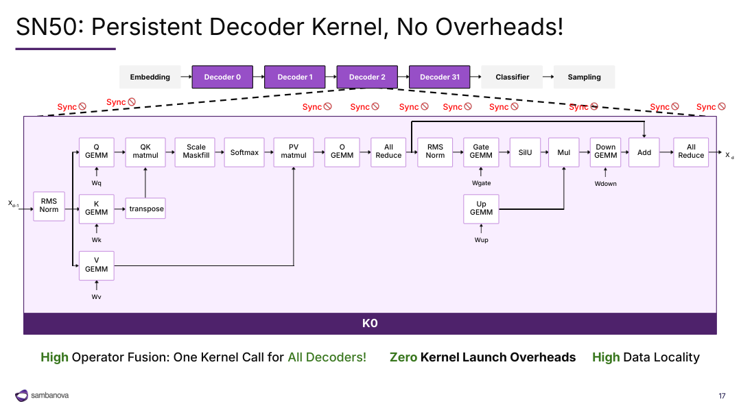
- The top row shows successive decoder layers. The enlarged box follows the operations inside one layer, from attention calculations on the left to the feed-forward calculations on the right.
- A kernel is a program launched on the accelerator. The purple K0 bar represents one persistent program connecting these operations, reducing repeated launches of separate small kernels.
- The compiler arranges where operations run and where their data goes. A completed intermediate result can pass through local memory to the next operation.
- Dependencies still apply. For example, softmax must receive the attention scores before it can calculate the weights used by the next operation. Keeping the program running does not mean every operation can run at once.
Load the next piece while computing the current piece
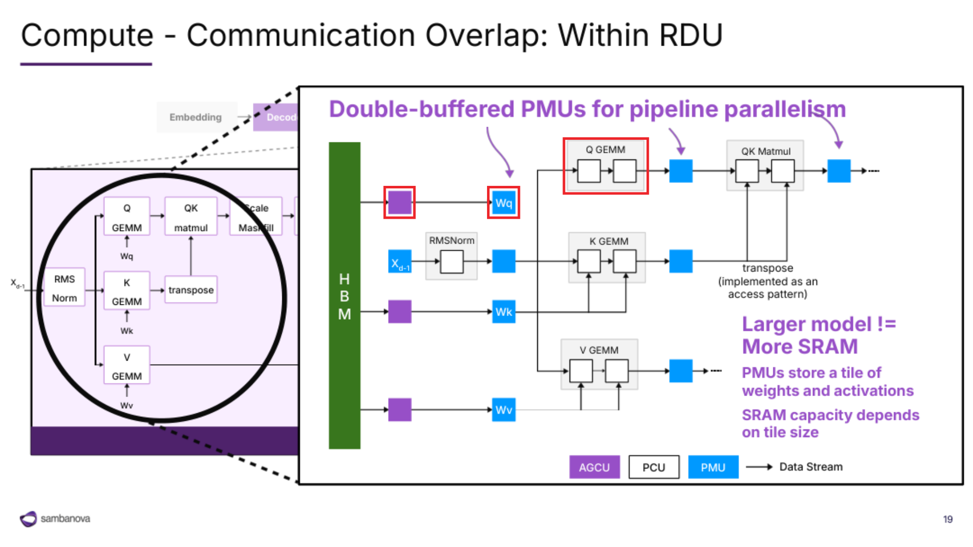
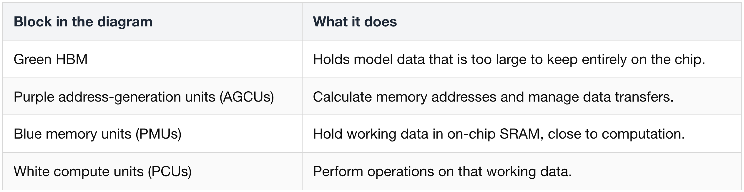
The three red rectangles mark an example address-generation unit, SRAM buffer, and group of compute units along the upper path.
- A tile is a small portion of a larger tensor. SN50 brings the tile it needs from HBM into SRAM.
- Double buffering provides two working buffers. Compute units read tile A from the first buffer while tile B loads into the second.
- When computation on A finishes and B has arrived, the compute units switch to B. The freed buffer can receive the next tile.
- For a hypothetical stage with a 4 µs load and 6 µs calculation, doing them consecutively takes 10 µs. Once the pipeline is running, loading the next tile during the current calculation can reduce the interval to 6 µs, assuming the two can proceed independently.
- This is what overlap means here: load B while computing A. If the next load takes longer than the current calculation, some waiting remains.
The whole model does not need to fit in the SRAM. Only the working tiles and retained intermediate results need space there.
Pause a producer when its output buffer fills
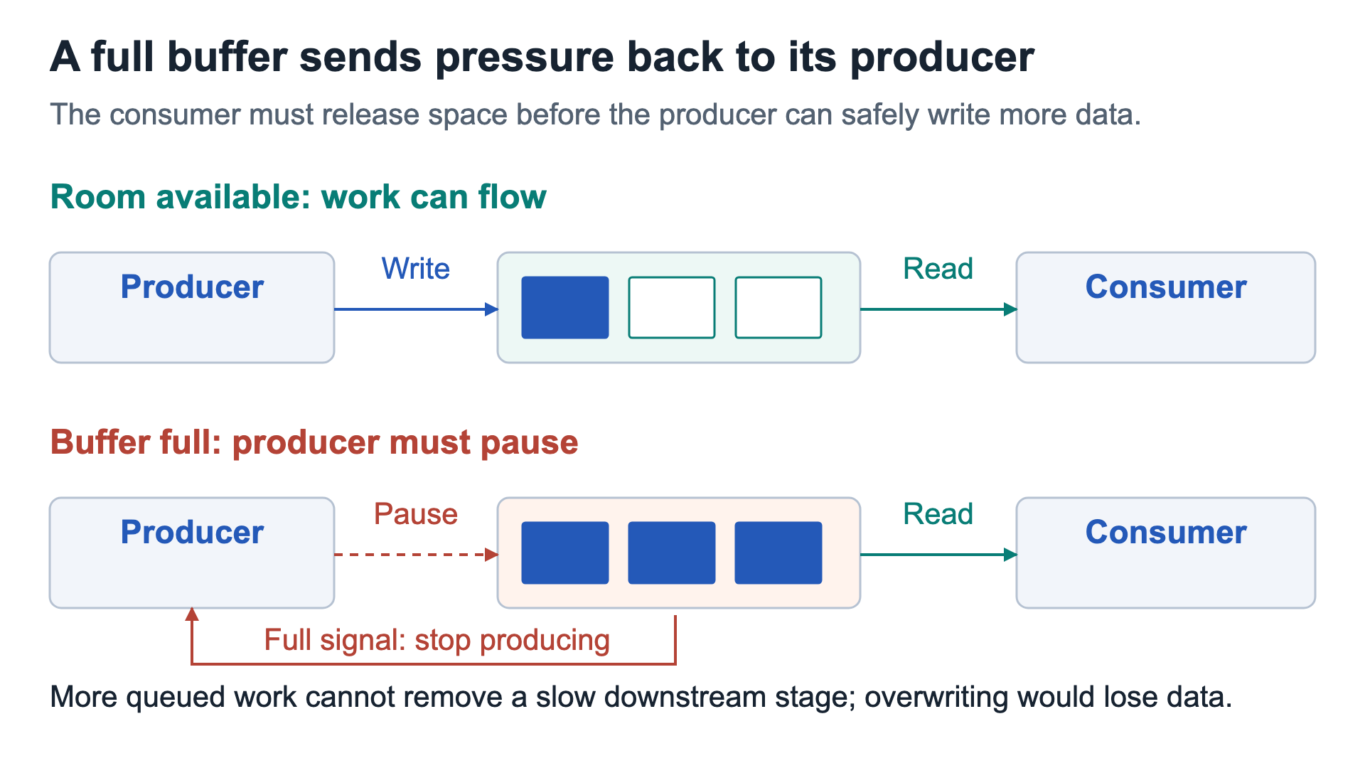
- In the upper row, the producer computes a result and writes it into a buffer. The consumer reads that result for the next operation.
- If the consumer falls behind, the buffer fills. The lower row’s red feedback path tells the producer to pause, preventing it from overwriting unread results.
- Once the consumer frees space, the producer can resume. This feedback is backpressure.
- SN50 therefore responds to data arrival and available buffer space. The LPU discussed earlier instead relies on a schedule that plans execution times in advance.
Why saving HBM transfers matters
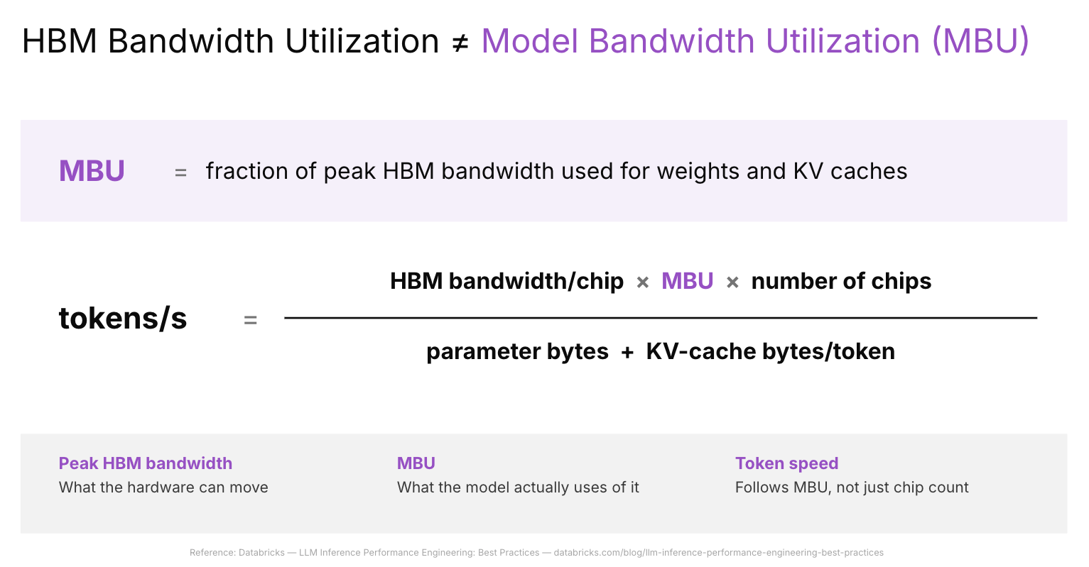
- Model bandwidth utilization (MBU) measures the share of peak HBM bandwidth used for weights and KV data. Intermediate-result traffic can keep HBM busy without increasing MBU.
- Hypothetically, 10 TB/s of peak bandwidth at 40% MBU delivers 4 TB/s of model data. Keeping intermediate results in SRAM leaves more bandwidth available for those model reads.
- In the figure’s simplified memory-limited formula, useful bytes per second are divided by required bytes per output token. Bandwidth alone is not token speed: the model, context length and data reuse affect the bytes required.
2) Split a calculation across chips, then combine the results
Use close connections for chips working on the same calculation
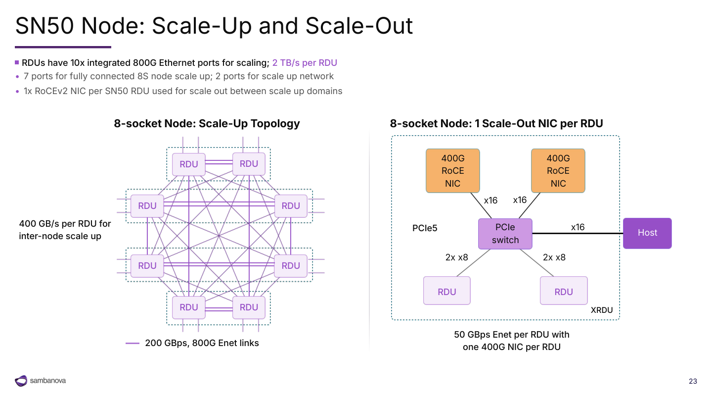
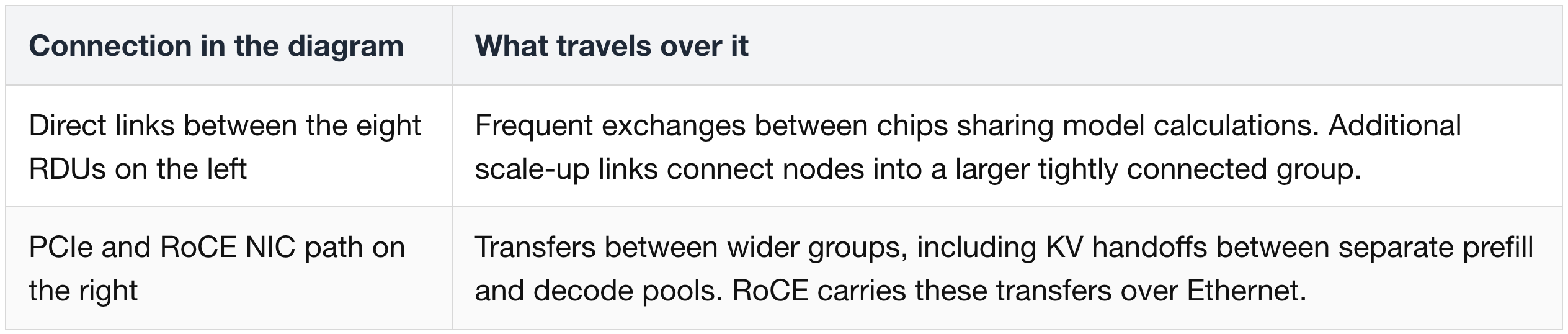
Tensor parallelism divides one large tensor calculation among several chips. Each chip calculates its assigned part, then exchanges the results needed to continue.
Combine partial results without an HBM round trip
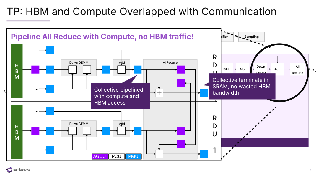
- The upper and lower rows represent two RDUs. Each performs its local matrix multiplication, labeled Down GEMM. GEMM means general matrix multiplication.
- Follow the arrows into AllReduce on the right. This operation combines corresponding partial results and makes the combined result available to the participating chips.
- As a simplified example, one chip contributes 2 and another contributes 3 to the same output value. A sum reduction produces 5, which the next operation needs.
- The blue SRAM buffers receive the exchanged results. The exchange does not require writing each intermediate result into HBM and then reading it back out.
- While a finished tile’s result is being exchanged, another tile can calculate or load its weights if it does not depend on that result. An operation that needs the combined value of 5 still waits for it.
The overlap operation is possible between different ready pieces of work. A calculation cannot use a result that has not arrived.
Check what the measured benchmark actually shows
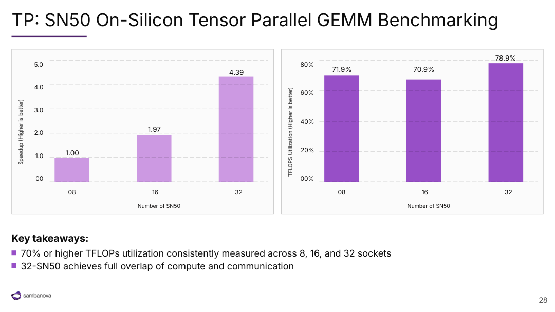
- Both charts put RDU count on the horizontal axis. The left measures speed relative to eight RDUs. The right measures achieved arithmetic performance as a percentage of peak compute performance.
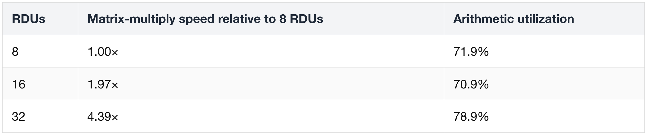
- Going from 8 to 32 RDUs supplies four times the chips. The higher utilization also contributes to the measured 4.39× speedup.
- This is a measured matrix-multiply kernel result. It does not establish 4.39× faster output from a complete language model.
3) Send each token’s data to the chips holding its selected experts
In a mixture-of-experts (MoE) layer, a router selects which expert networks process each token. Expert parallelism places different experts on different chips. The system must therefore move each token’s working data to the chips holding its selected experts.
Selective dispatch: choose the destination, then send
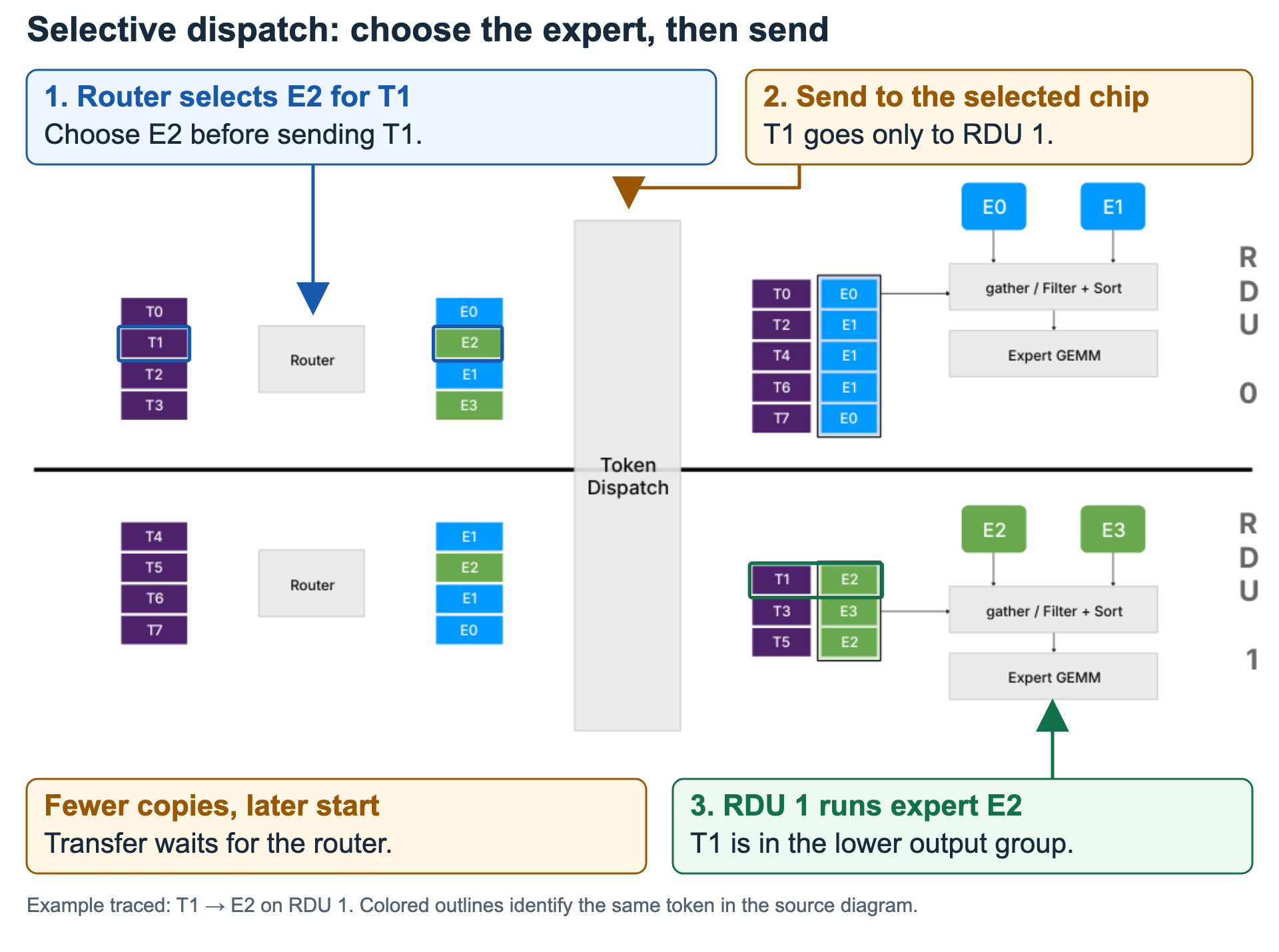
- The upper chip, RDU 0, holds experts E0 and E1. The lower chip, RDU 1, holds E2 and E3.
- Follow T1 in the upper-left group. Its router chooses E2, shown in green.
- Dispatch sends T1’s data to RDU 1, where E2 resides. T1 appears in the lower-right group and enters the expert calculation there.
- Sending only the selected data avoids unnecessary copies. However, dispatch must wait until the router identifies the destination, then group the data for delivery.
Broadcast: send early, then keep only the selected data
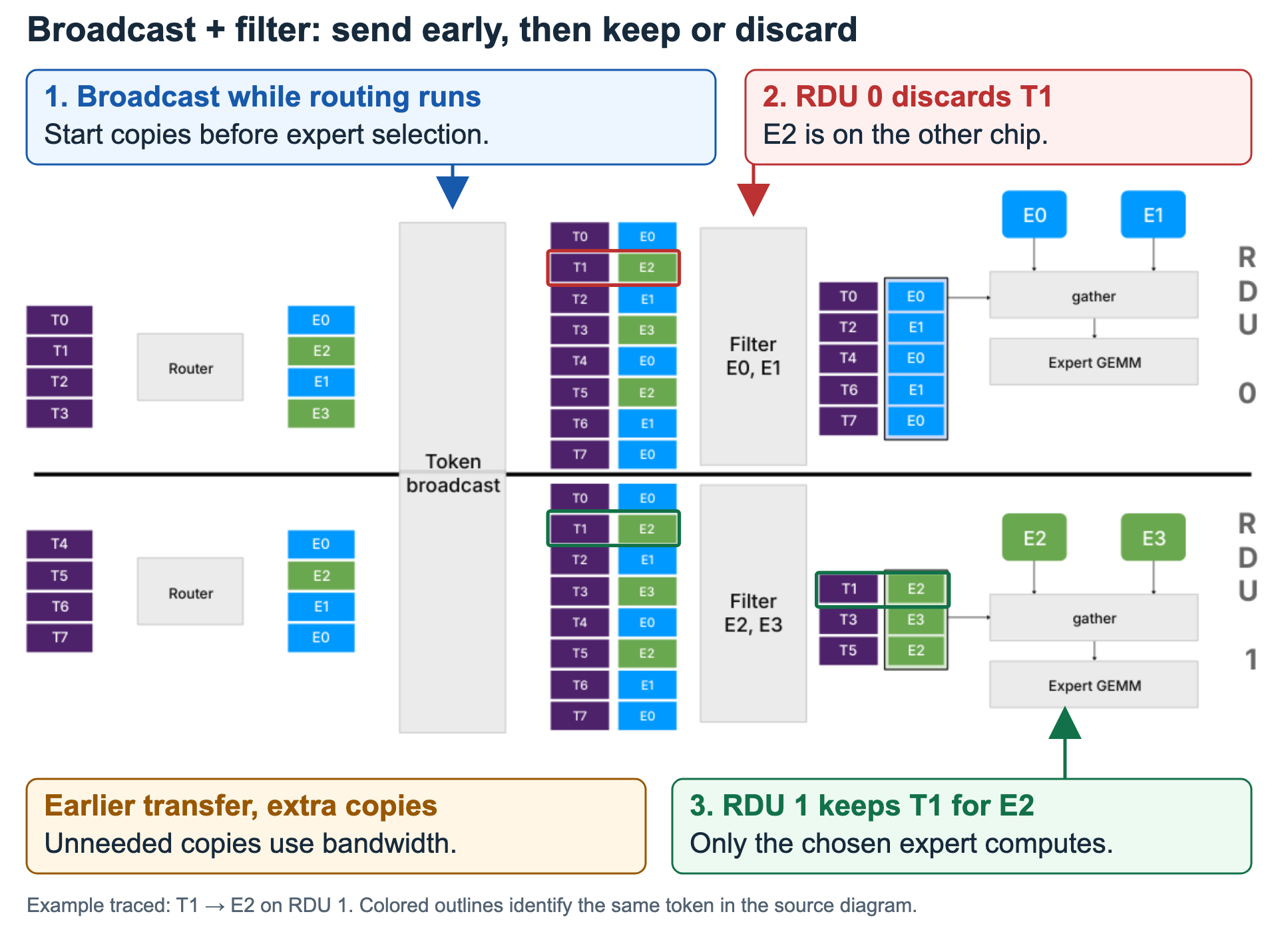
- In this two-chip example, broadcast sends the token data to both expert groups. The copies can start moving while the router is still choosing experts.
- Once the choices are known, each destination filters its received data. For T1 → E2, RDU 0 discards its copy and RDU 1 keeps the copy for E2.
- Expert computation still needs the routing decision. Broadcasting the input does not make every expert process every token.
- This can reduce the wait after routing finishes, because the input may already be at its destination. The cost is transmitting and filtering extra copies.
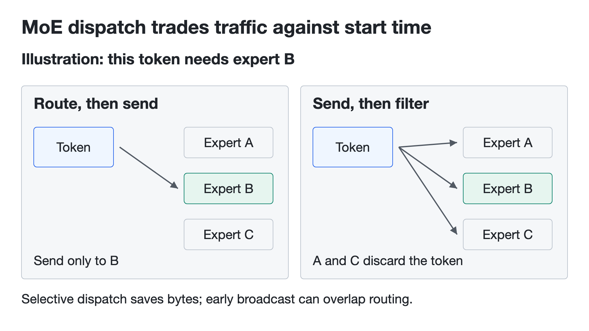
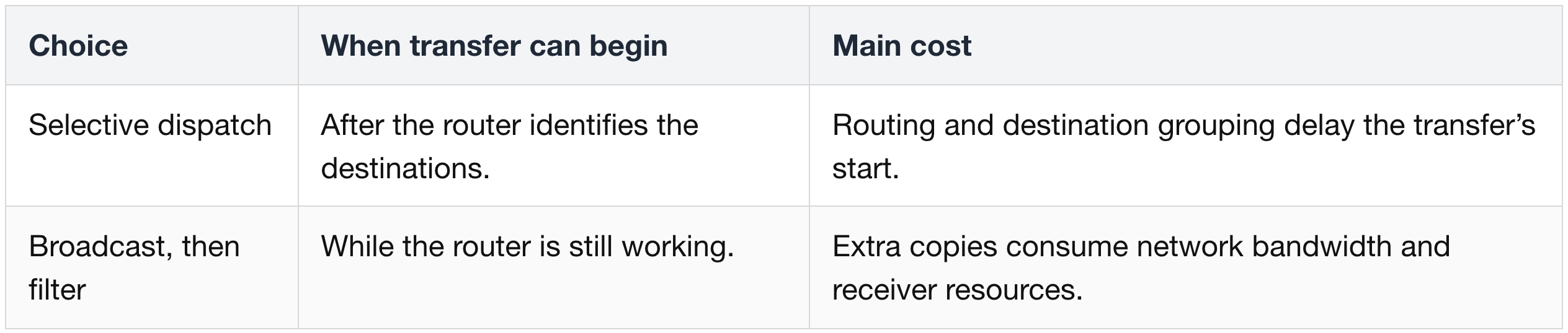
Broadcast helps only when the earlier transfer saves more time than the extra traffic costs. With more destinations, the number of copies can make it less attractive.
4) Distinguish model-speed projections from memory requirements
More chips provide more bandwidth, but speed does not necessarily rise in proportion
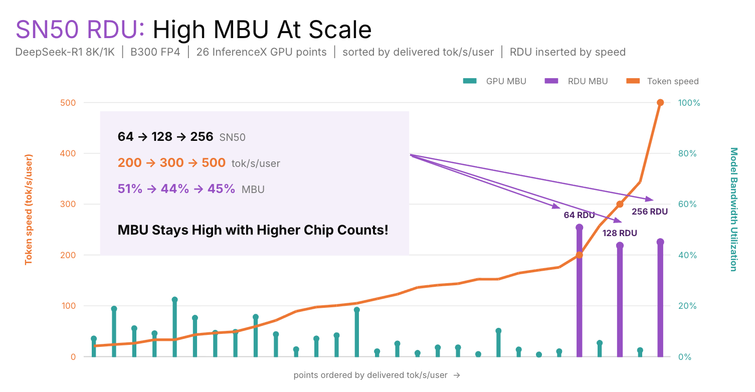
The blog labels the SN50 points as modeled, for DeepSeek-R1 with 8K input and 1K output tokens:
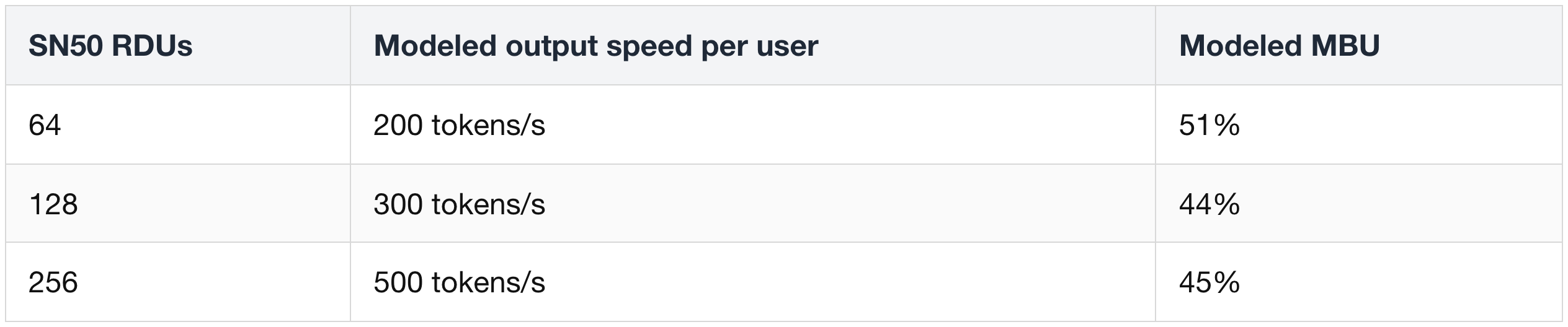
- The orange line uses the left speed axis. Purple RDU and teal GPU markers use the right MBU axis.
- Horizontal positions rank configurations by speed; they are not time or chip count.
Enough memory to hold the model does not mean enough bandwidth to serve it quickly
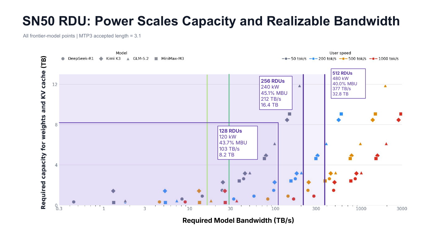
- The vertical axis is the memory capacity needed for weights and KV cache, in TB. Higher points need more storage.
- The horizontal axis is the model-data bandwidth needed, in TB/s, on a logarithmic scale. Points farther right need faster data delivery.
- Shapes identify models. Gray, blue, orange and red identify targets of 50, 200, 500 and 1,000 tokens/s per user, respectively.
- Each purple system boundary has a capacity ceiling and a bandwidth ceiling. A workload must fall below the top and left of the right edge to fit both. The larger systems’ capacity ceilings extend above the plotted vertical range, so use the values in their labels.
For a hypothetical workload needing 6 TB of capacity and 150 TB/s of model-data bandwidth:
- The plotted 128-RDU system has 8.2 TB of capacity but only 103 TB/s of model-data bandwidth. The data fits, but the system falls short of the bandwidth requirement for that speed.
- The plotted 256-RDU system has 16.4 TB and 212 TB/s, meeting both requirements in this model. Its stated power also rises from 120 kW to 240 kW.
Capacity doubles with chip count in these examples, while usable bandwidth also depends on utilization. From 256 to 512 RDUs, capacity doubles but model-data bandwidth rises from 212 to 377 TB/s, about 1.78×. A workload can therefore fit in memory yet miss its target token speed.
5) Assign prompt processing, output generation, and reusable KV storage to separate pools
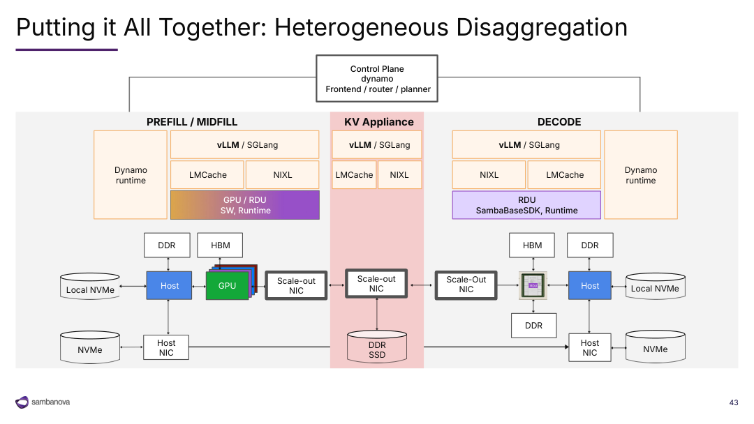
The diagram separates three jobs:
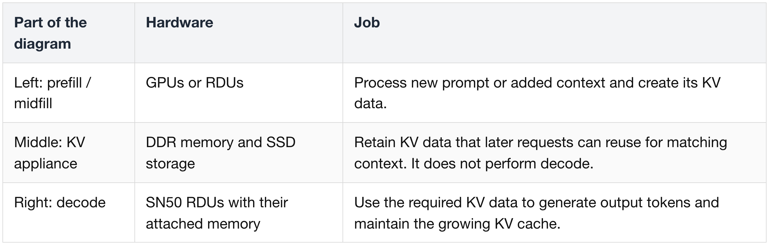
For a request whose prompt has not already been cached:
- First, the left pool processes the prompt and produces its KV data.
- Next, the transfer path delivers the required KV data to the right pool. The decode work that uses it must wait until it arrives.
- The SN50 pool then generates output tokens. The prefill pool becomes available to process another prompt.
- Reusable KV data can be retained in the middle appliance. A later request with matching context can reuse that portion instead of recomputing it. The appliance is not a requirement to store every request’s KV data before decode.
The control plane chooses where requests run. The software boxes below provide model execution, cache management and transfers. The network-interface cards (NICs) carry data between pools.
Separating prefill and decode into different pools lets an operator add capacity where demand is higher. However, the required KV data must move between them, and decode waits if it arrives late. This arrangement can improve hardware utilization and total serving capacity, but it speeds up an individual request only when the time saved exceeds the added transfer waiting.
5. Hyperscalers specialize around their own workload and system constraints
(1) Google TPU 8: inference and training justify different networks
1) Shorten inference communication inside the package
- Google (NASDAQ: GOOGL) separates inference-oriented TPU 8i from training-oriented TPU 8t.
- During token generation, the next calculation often waits for the preceding result. Shorter memory and communication delays can therefore make each user's output arrive faster.
- Training must sustain calculations and exchanges across larger groups while holding the model and training state. That places more weight on memory capacity and sustained communication bandwidth.
- TPU 8i and TPU 8t allocate memory and network resources differently to address these demands.
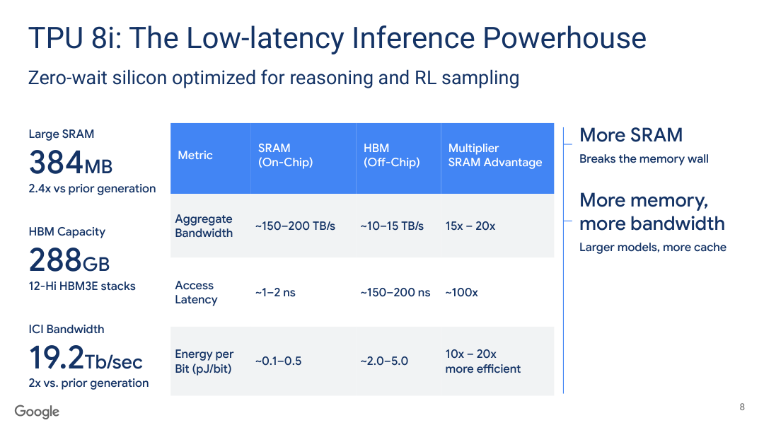
- The table compares aggregate bandwidth, access latency, and energy per bit for SRAM and HBM.
- The 384 MB SRAM working store is far smaller than the 288 GB HBM capacity, but it can serve repeatedly used local data through faster, lower-energy paths. Keeping a useful tile or intermediate there avoids another HBM access.
Shorten the collective path as well
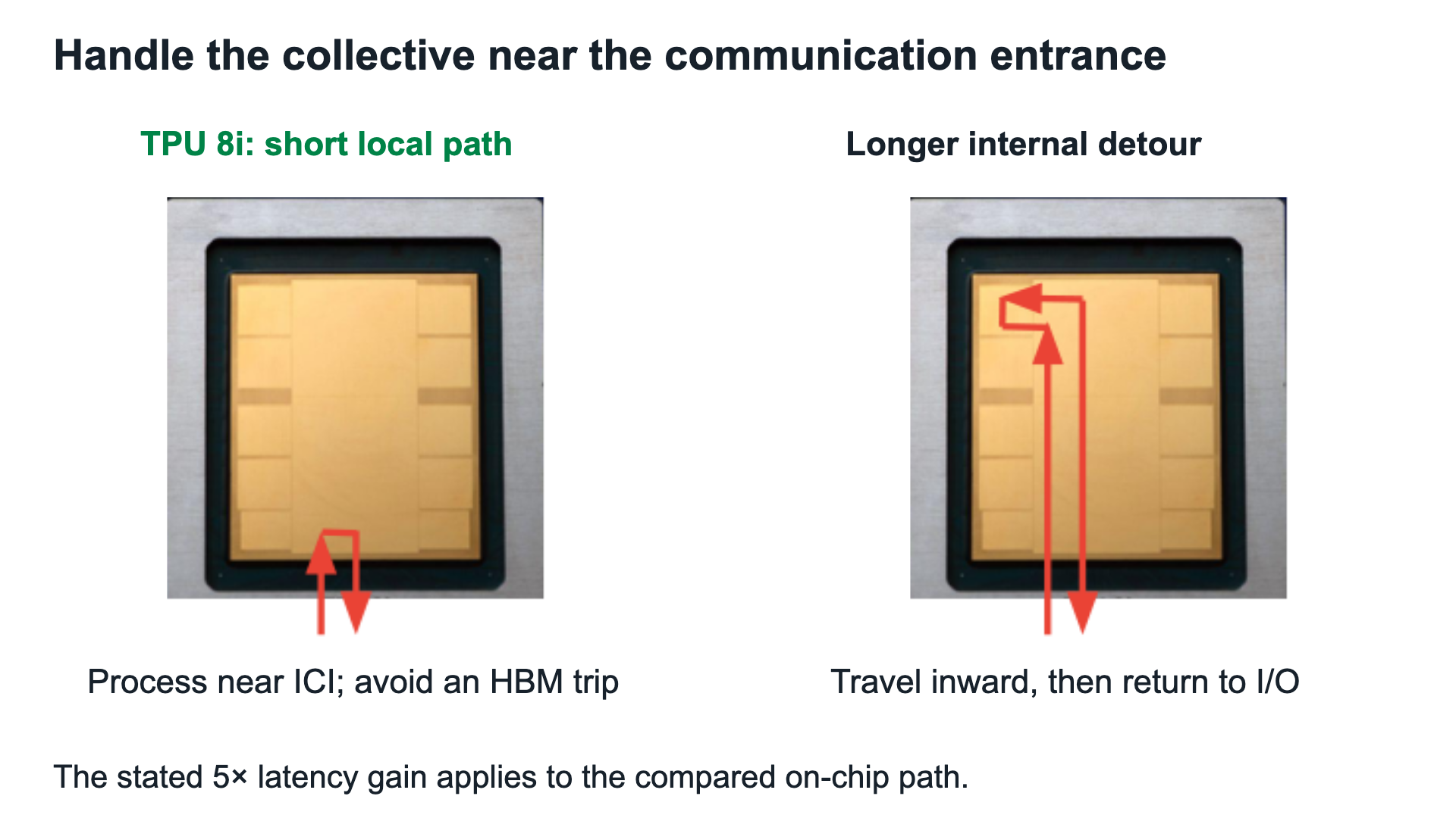
- The short red path on the left handles the collective near the communication interface. The longer path on the right carries data farther into and back out of the package. The block diagram below shows where the new collective engine sits.
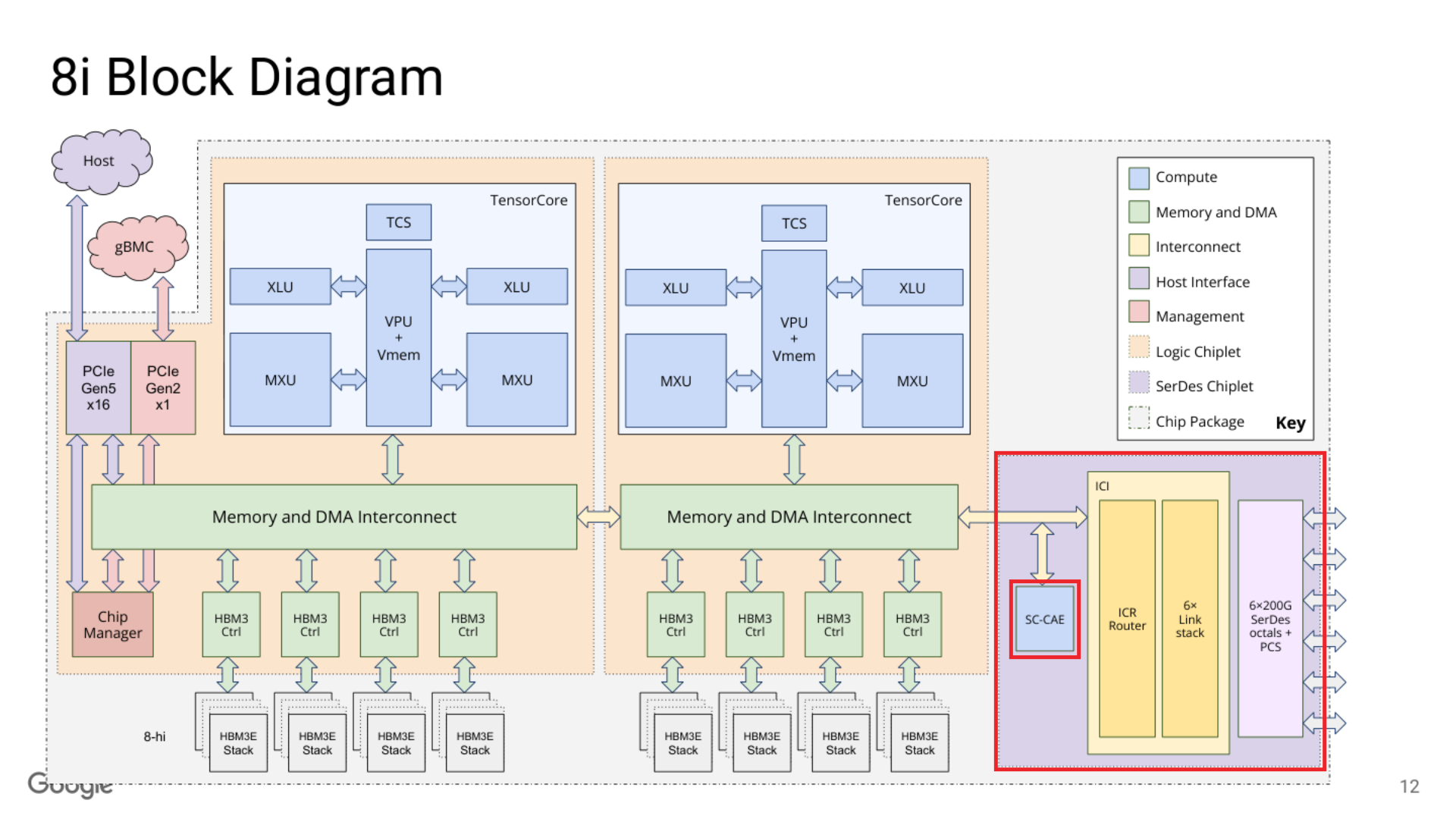
- The peach logic chiplets perform tensor computation.
- The large red box surrounds the purple communication chiplet, including the ICI interface that connects this TPU to other TPUs.
- The small red box locates the nearby SC-CAE engine, which handles collective operations such as combining partial results from several devices.
- Placing that work near the communication entrance avoids an extra trip deeper into the package and HBM before sending data onward.
- Processing the collective at the communication interface lets the result move onward without that internal detour.
- The disclosed 5× latency claim applies to that shortened on-chip path. The end-to-end collective also uses external links and other devices, so the same factor cannot be assigned to every pod-wide exchange or complete model.
2) Reduce route length across the inference pod
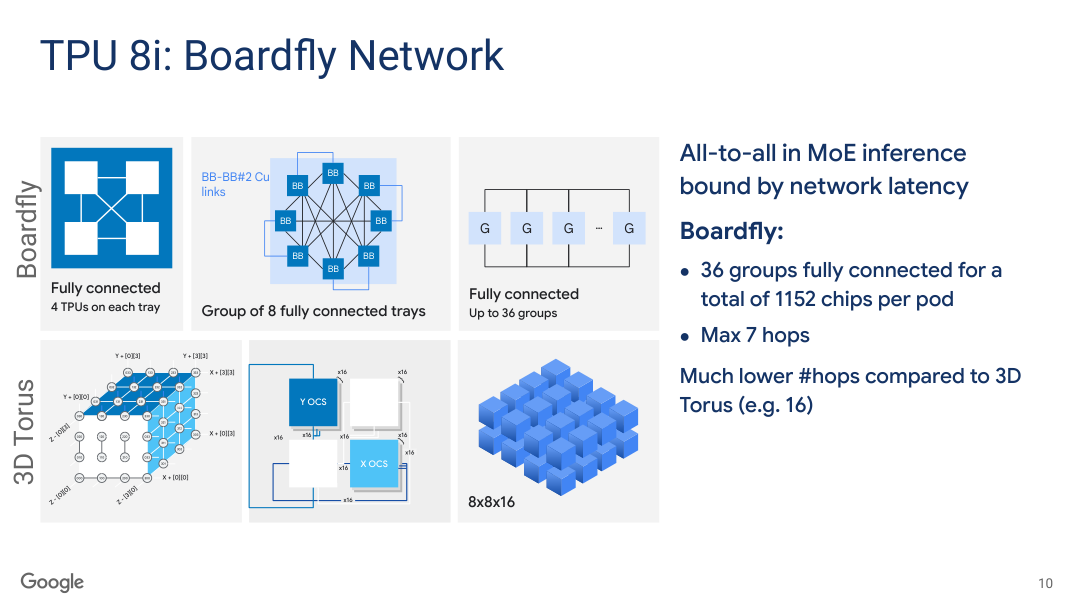
- The upper row builds a pod of up to 1,152 TPUs from connected trays and groups.
- The lower row compares a torus network, where devices connect to neighboring devices in a grid with wraparound links.
- The stated maximum falls from 16 → 7 hops in the shown examples.
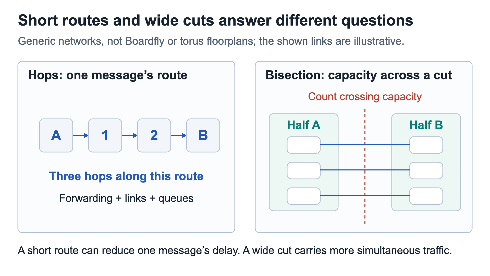
- The left panel follows one three-hop route. The dashed cut on the right separates equal groups and exposes the links carrying traffic between them. These are generic teaching networks.
- A hop is one step along a message's network route. Each step adds handling and link delay, while a busy route can also add queueing time.
- MoE all-to-all exchanges send token activations to devices holding the selected experts. Reducing their route length can help the dependent expert work start sooner.
- The actual delay still depends on forwarding costs and congestion, so 7 versus 16 hops does not establish the same ratio in application speed.
3) Balance training memory and sustained communication
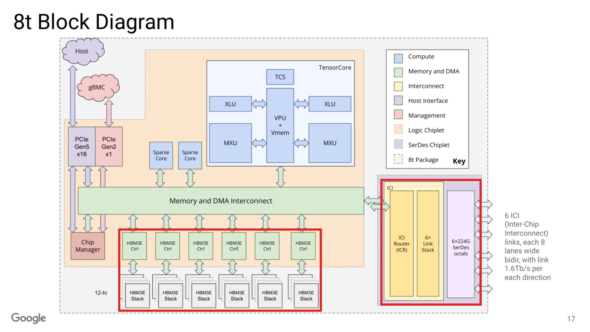
- TPU 8t combines different resources for different training tasks:
- Dense tensor units perform regular matrix operations.
- SparseCore blocks handle less regular data access.
- The lower red rectangle marks six local HBM interfaces.
- The right rectangle marks six separate ICI links, supplying 1.2 TB/s one-way between devices.
- Training can require many devices to exchange results at once.
- Bisection bandwidth measures link capacity across an equal split of that network, helping describe how much concurrent traffic can cross it.
- The training torus emphasizes sustained communication capacity; the inference design emphasizes shorter routes.
- Training uses mixed precision:
- An FP4 peak does not imply that routing or gradient reductions use FP4 throughout.
- Higher-precision stages remain part of the mixed-precision training process developed with model teams.
4) Reconfigure working groups after a failure
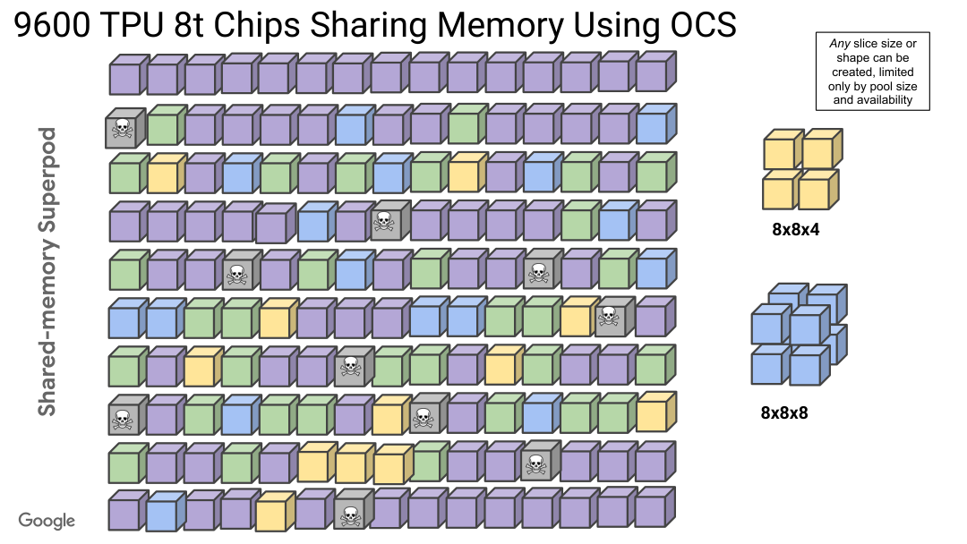
- The colored blocks are groups available to form a job slice. Skull-marked blocks have failed.
- Optical circuit switches (OCS) reconnect working groups into a replacement slice.
- The job resumes from saved checkpoint state on those resources.
- Rebuilding the connections restores usable hardware. It does not recreate work lost since the checkpoint.
5) Make the hardware accessible and use AI to optimize its implementation
Map model code onto specialized resources
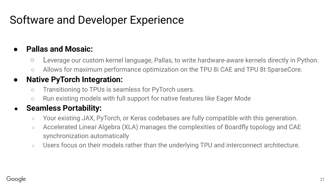
- Through the framework path, a developer supplies model operations and lets the compiler assign work and communication to TPUs.
- For a slow, performance-critical kernel, Pallas and Mosaic provide more direct control over where working data sits and how specialized engines execute it. This lets developers tune selected operations without manually programming the entire model.
Optimize defined blocks within the chip-design process
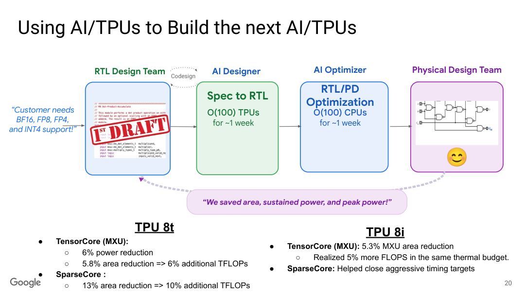
- RTL, or register-transfer level, specifies how a digital circuit moves and transforms data.
- Google’s TPU team works with Google DeepMind on this optimization loop. It proposes circuit changes, checks that they preserve the required function, then evaluates physical placement and wiring.
- The TPU 8t matrix-unit result lists 6% lower power and 5.8% less area for that block.
- A smaller matrix unit leaves chip area for other circuitry or more compute. A lower-power unit draws less power and produces less heat while doing its work.
- Those percentages apply to the named circuit blocks, not the entire chip.
(2) OpenAI Jalapeño: make the common path local and compare at the required speed
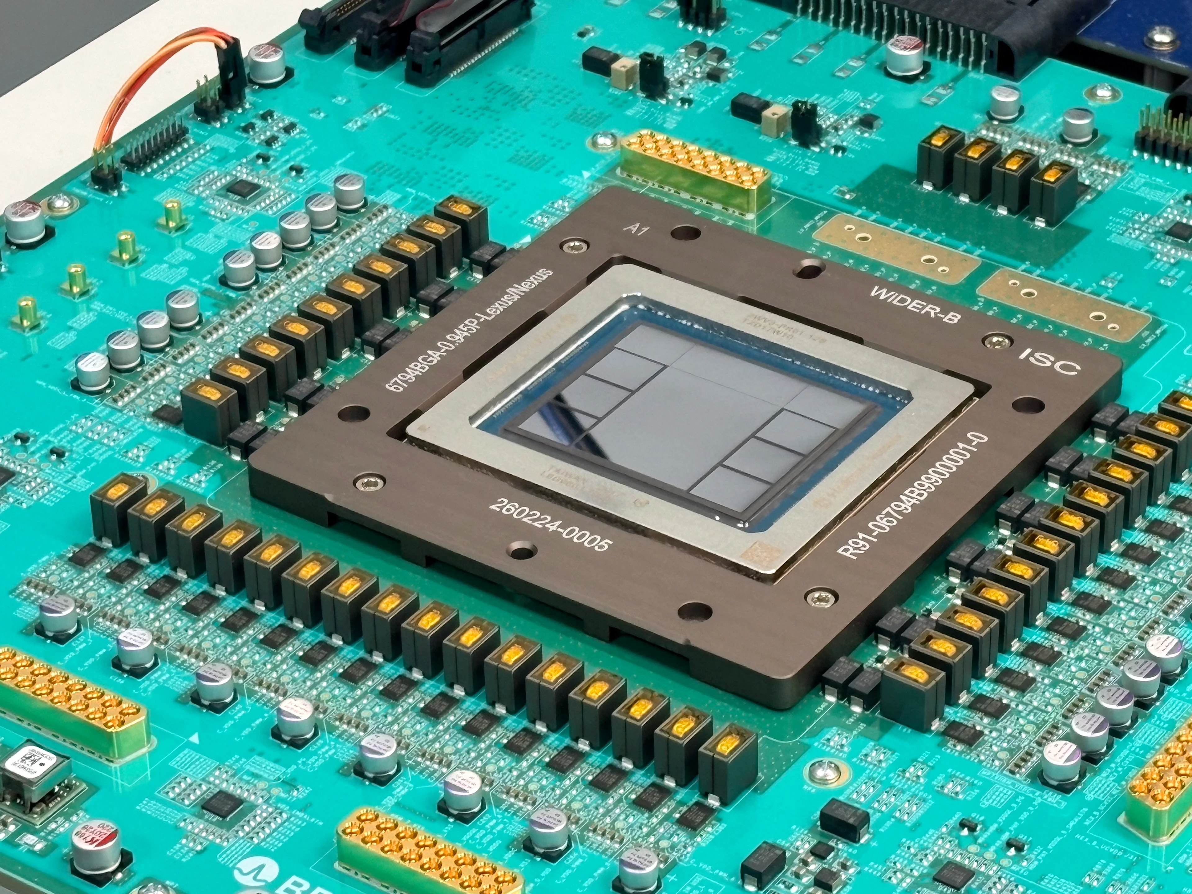
Jalapeño combines two approaches to reducing inference delays:
- a) place frequently used data beside the processors that need it,
- b) and run prefill, drafting and verification on hardware that supports all three phases.
This lets software change the work assigned to the accelerator while retaining useful model state locally. The following sections explain the data paths, resource allocation and measurements behind those choices.
- OpenAI names Broadcom and Celestica (NYSE: CLS) as development partners. Their disclosed roles cover different parts of delivery:
- Broadcom said in September 2026 that it had shipped Jalapeño during fiscal Q3.
- Celestica described its systems role with OpenAI and Broadcom, with initial custom-rack deliveries expected in 2026 and mass production planned for 2027.
1) Follow what must finish before the next calculation starts
Generating a token involves a sequence of dependent calculations. A later calculation cannot start until the earlier one has produced and delivered the input it needs.
Read the example from left to right:
- The blue earlier layer produces an activation, an intermediate result used by the next layer.
- The red required transfer carries that result to where the next calculation will run.
- The green later layer starts its dependent calculation only after that input arrives.
Other independent work can run during the transfer. It cannot remove this particular dependency: the later layer still needs the earlier result.
- Adding up all memory interfaces’ bandwidth does not measure how quickly this sequence finishes. Its required input may use one busy path while other paths are idle.
- Weight reads are only part of the sequence. The system also reads KV data, transfers intermediate results and combines contributions from cooperating processors.
- Jalapeño’s placement and communication mechanisms aim to shorten these specific reads and handoffs. Their effect depends on whether software puts the work and data on the intended paths.
2) Follow the data inside one chip, then between chips
Keep frequent reads local and give repeated exchanges a suitable communication path.
Inside one chip
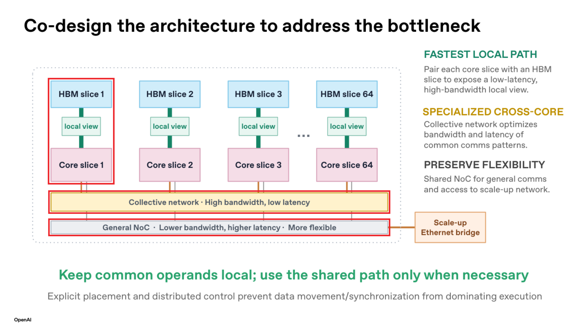
- The vertical red box marks a core slice (a group of processing resources) paired with its local HBM slice. Horizontal red boxes mark the two networks.
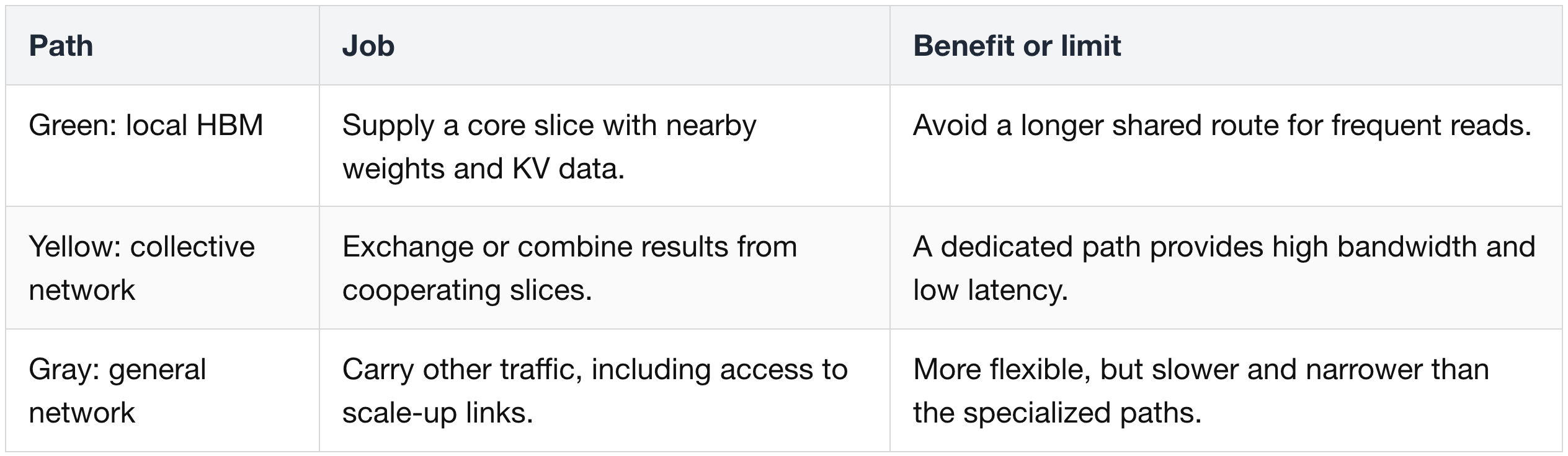
Software places data and work. Each slice reads its data, computes, then exchanges any required results; dependent work waits for those results.
Prefetch the next input
- Prefetching requests block B while the core computes with block A, provided B’s load does not depend on A’s result.
- If B arrives before it is needed, the next calculation avoids that load wait.
Between chips
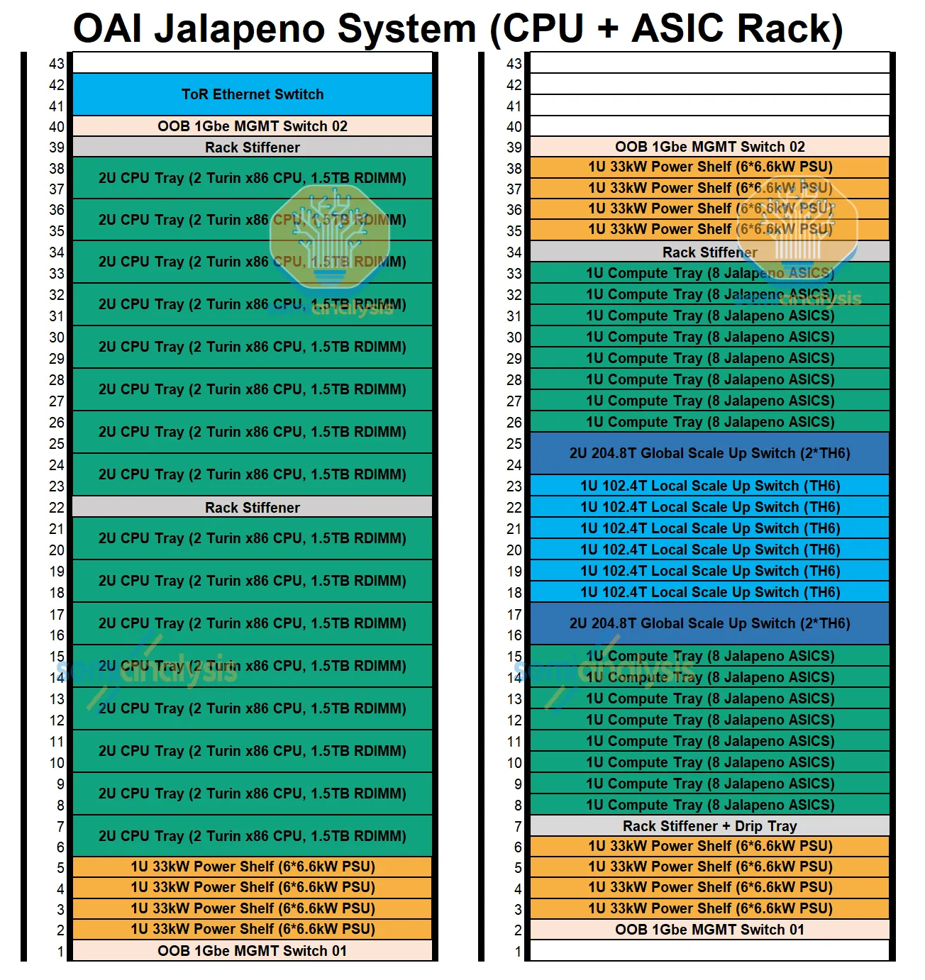
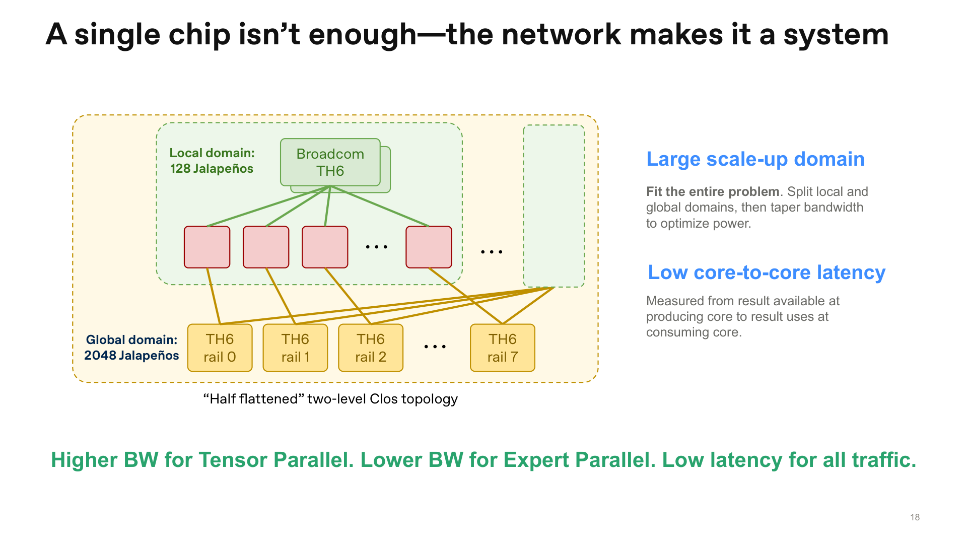
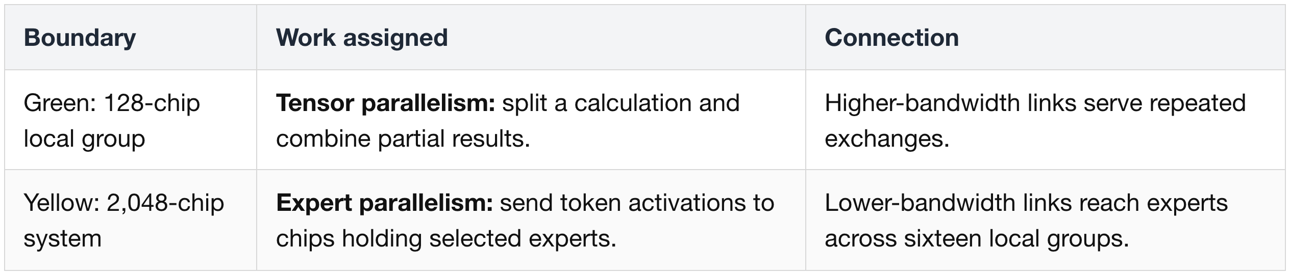
- “Local” here means the 128-chip group, not an HBM slice inside one chip. Eight chips per tray × sixteen trays form each group.
- SemiAnalysis reports 600 GB/s of one-way local communication per chip, plus 200 GB/s per chip for the wider domain. These are separate budgets, not equally fast access to every chip.
- Broadcom Tomahawk 6 (TH6) switches carry both local and wider traffic; the lower rails connect the groups.
3) Adjust resource use as inference moves between phases
Changing phase demand can leave fixed processor pools idle or overloaded.
What each phase needs
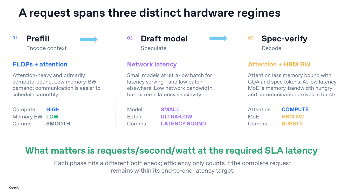
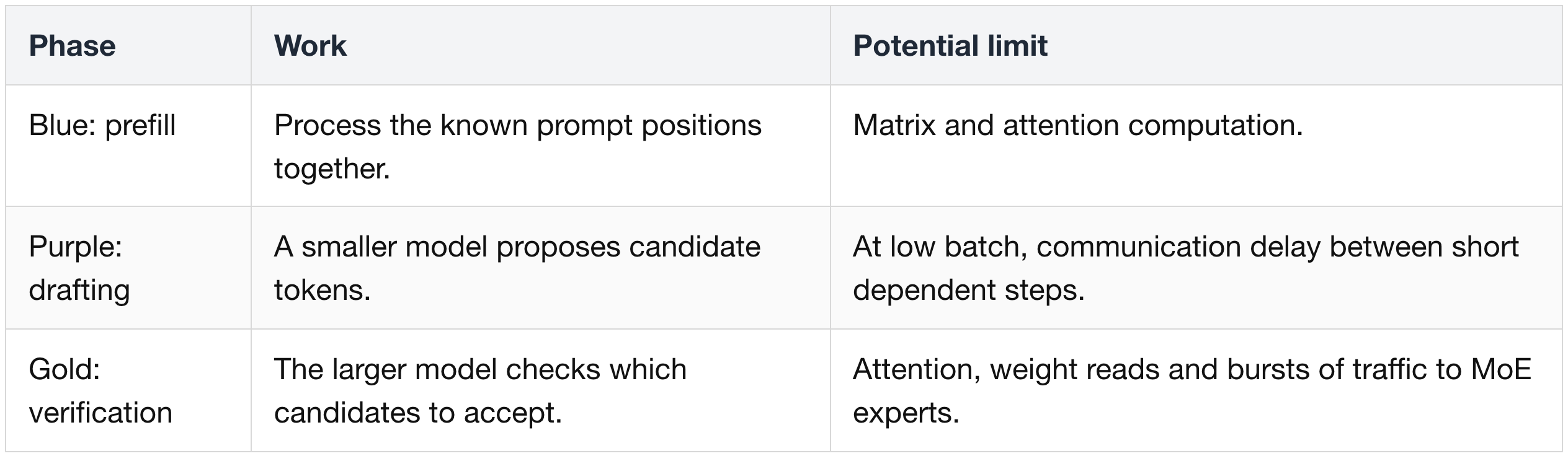
Prompt length and draft acceptance change the balance between these phases.
Fixed assignments versus reusable hardware
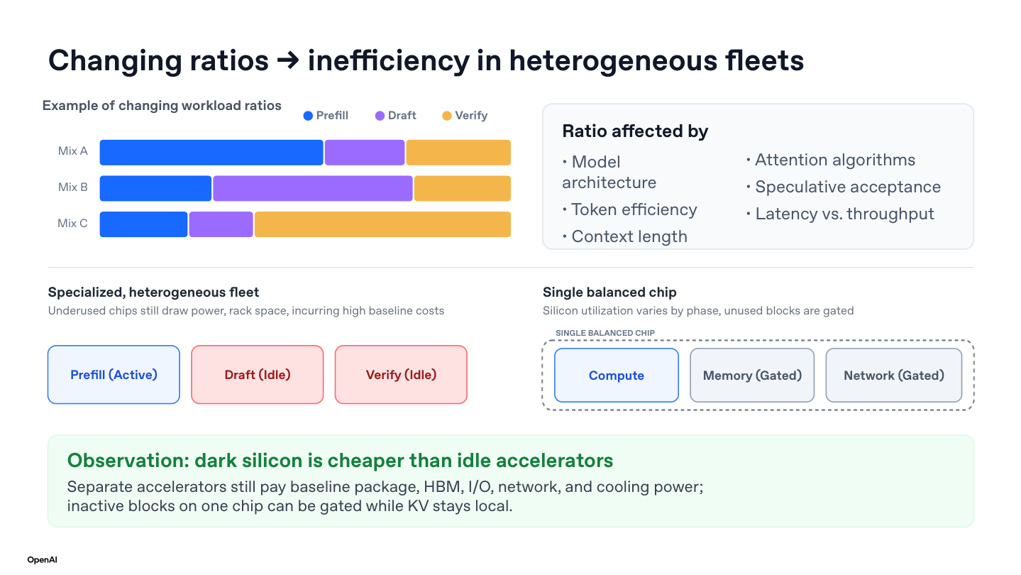
- Top: Blue, purple and gold show prefill, drafting and verification. Mixes A, B and C emphasize different phases; the proportions are illustrative.
- Lower left: Processors assigned to inactive phases sit idle.
- Lower right: One accelerator supports multiple phases and retains useful state locally. Gated blocks reduce or stop activity but still occupy chip area.
- Reassignment can reduce queues and idle capacity, subject to memory, software and transfer requirements. Separate pools can also work efficiently when capacity matches demand and transfers overlap useful work.
The same issue across a fleet
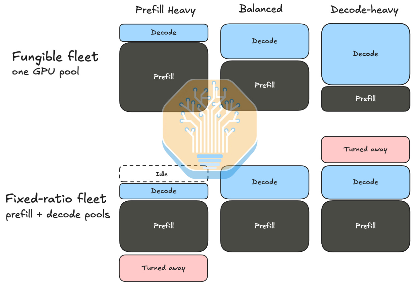
In this generic example, gray is prefill and blue is decode:

Fungible means resources can change roles. GPU fleets can also resize software-defined pools when the hardware supports both phases.
4) Compare total throughput at the same per-user output speed
Choose a per-user speed, then compare total throughput at that speed. Peak throughput and maximum user speed are different operating points.
OpenAI’s Jalapeño chart
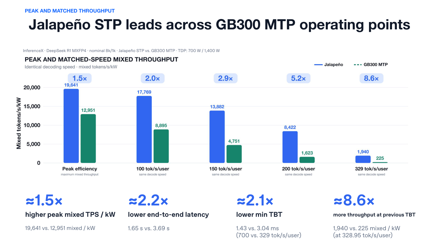
- Vertical axis: Mixed input-plus-output tokens/s/kW of chip-package design power, not output alone or whole-rack power.
- Blue: Jalapeño with single-token prediction (STP). Green: GB300 with multi-token prediction (MTP).
- Test: DeepSeek R1 MXFP4, nominal 8K input / 1K output; 700 W Jalapeño and 1,400 W GB300 design-power denominators. OpenAI published this chart in its Hot Chips presentation.
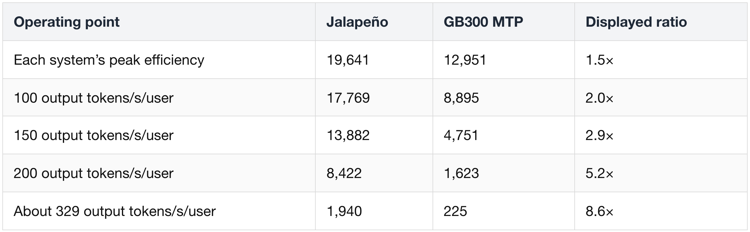
All throughput values use mixed tokens/s/kW. Faster per-user targets can require smaller batches, reducing weight reuse and total throughput. Both systems’ bars shrink, but GB300’s shrink faster: the rising ratio is a larger relative lead, not more total output at the faster target.
SemiAnalysis: Jalapeño throughput per utility megawatt
- OpenAI’s public STP tables use a different GB300 baseline from the MTP chart above.
- SemiAnalysis’s Jalapeño review adds the comparison below, using modeled utility power rather than chip-package design power.
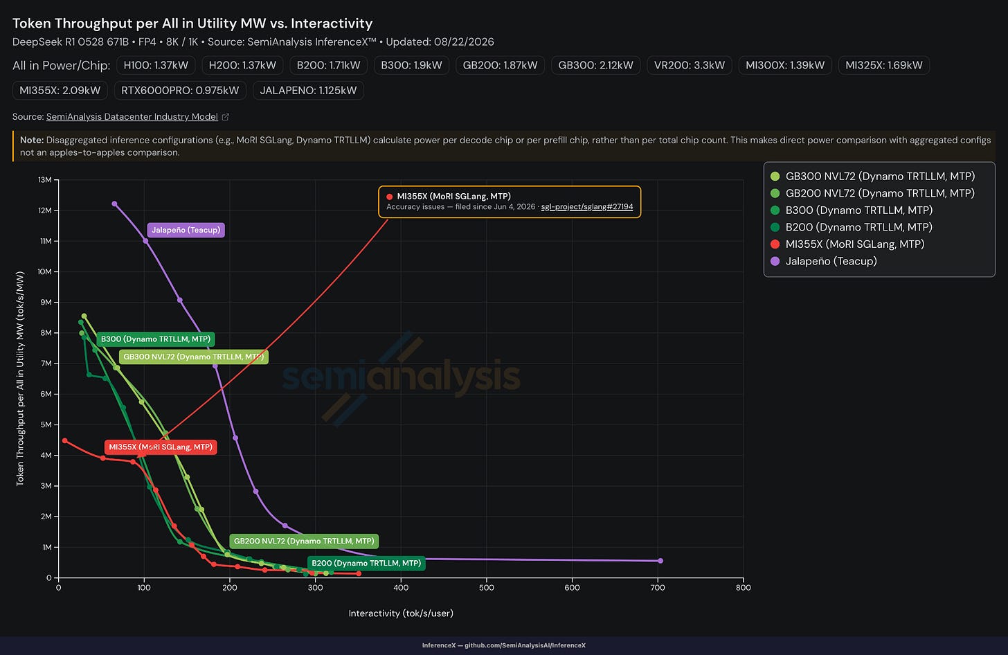
- Horizontal: Output tokens/s/user.
- Vertical: Combined input and output tokens/s per modeled utility MW. Both axes are linear; the workload is DeepSeek R1 0528 (FP4), with 8K input / 1K output.
- Purple: Jalapeño using STP.
- Green shades: NVIDIA GPUs using MTP. Red: AMD MI355X using MTP.
- Compare curve heights at the same user speed. Jalapeño’s higher purple curve reports more total token throughput per modeled MW over the shared speed range. Its roughly 700 tokens/s endpoint is one active request, not peak aggregate throughput.
- The chart flags different power accounting for split prefill/decode configurations and an accuracy issue with the AMD result. These conditions limit a direct efficiency ranking.
The Jalapeño numbers were supplied by OpenAI. SemiAnalysis witnessed selected lab runs, rather than independently reproducing the full suite.
5) Software: use AI to optimize kernels while preserving correct data handoffs
This subsection covers the software running on Jalapeño: AI helps improve kernel code so that the chip executes the calculations faster.
A kernel is a program for an operation or group of operations. Jalapeño’s kernels use Gluon, a lower-level programming interface in Triton, to control how work and data are assigned to the hardware.
TensorInfo records the data layout: which element is stored where. A later kernel must read the arrangement produced by the earlier one, or the program must convert that arrangement before it is used.
This control also requires model-specific programming. UBS argues that custom accelerators are most attractive when a large, relatively stable workload lets the operator reuse that software investment across many requests. Changing a model can require new kernels and another optimization pass.
A faster producer must still give its consumer the expected data
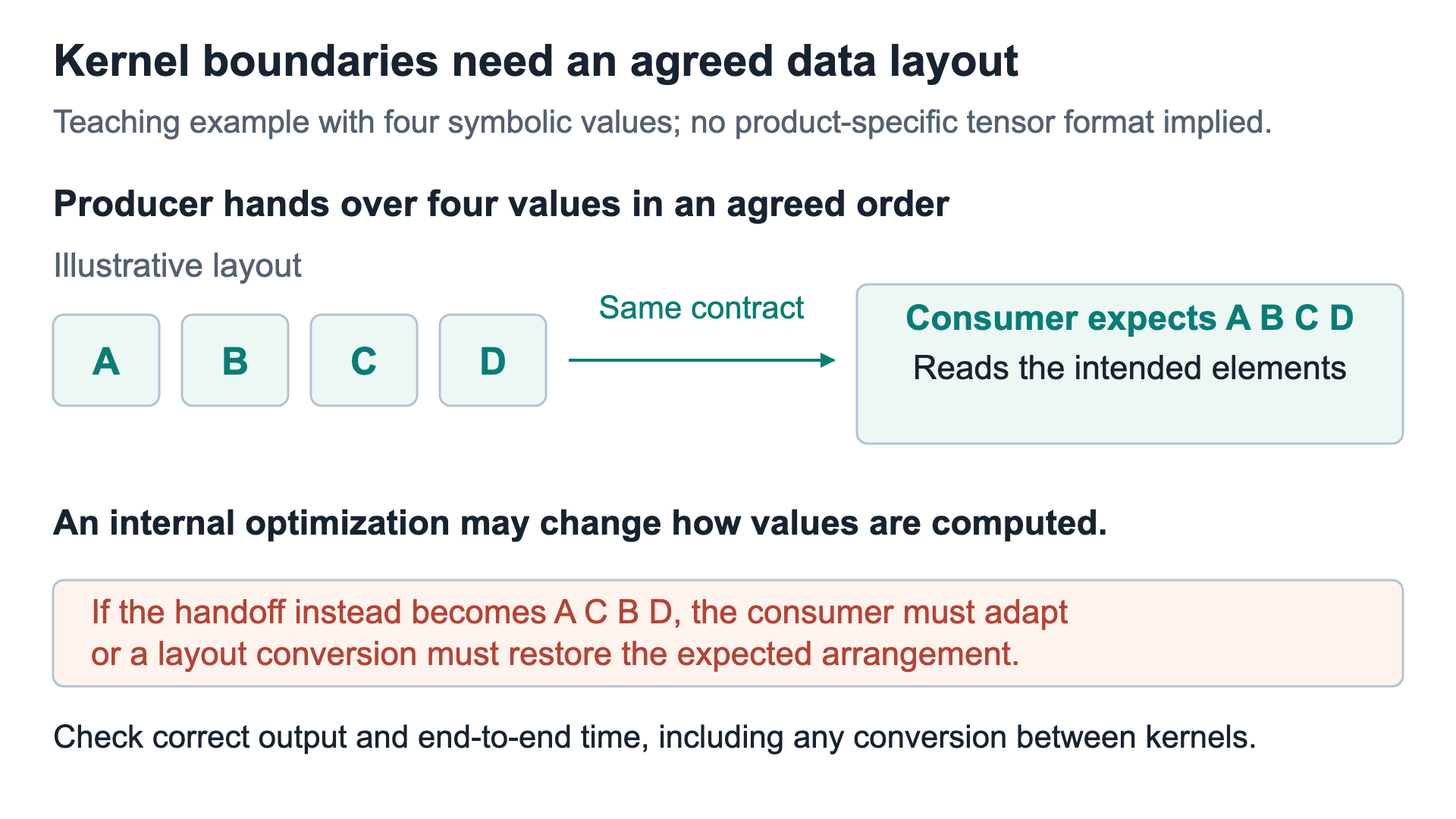
Both kernels run in sequence: Kernel 1 produces data that Kernel 2 needs for the next calculation. They perform different stages of the work.
Follow this illustrative handoff:
- Kernel 1 produces four values in the order A, B, C, D. Kernel 2 expects that order.
- A faster version of Kernel 1 stores the same results as A, C, B, D. If Kernel 2 reads them as before, it confuses B with C.
- To use the faster version, change how Kernel 2 reads the data or add an operation that restores the expected arrangement.
- Adopt the change only if Kernel 1, any rearrangement and Kernel 2 together still produce correct results and finish sooner.
A kernel optimization helps only if its time savings exceed any extra data movement or rearrangement it causes elsewhere in the model.
This is why the AI-assisted improvements in the next slide are checked in the complete execution path: making one kernel faster must translate into a faster model without changing the required results.
Use AI to improve a kernel through successive, tested code changes
- The chart shows AI improving a working kernel through successive code changes, with measured performance increasing as those changes are tested and refined.
- OpenAI says AI drove most of the optimization in this DeepSeek attention example, bringing the kernel from 0.31% to about 89% of its estimated performance ceiling.
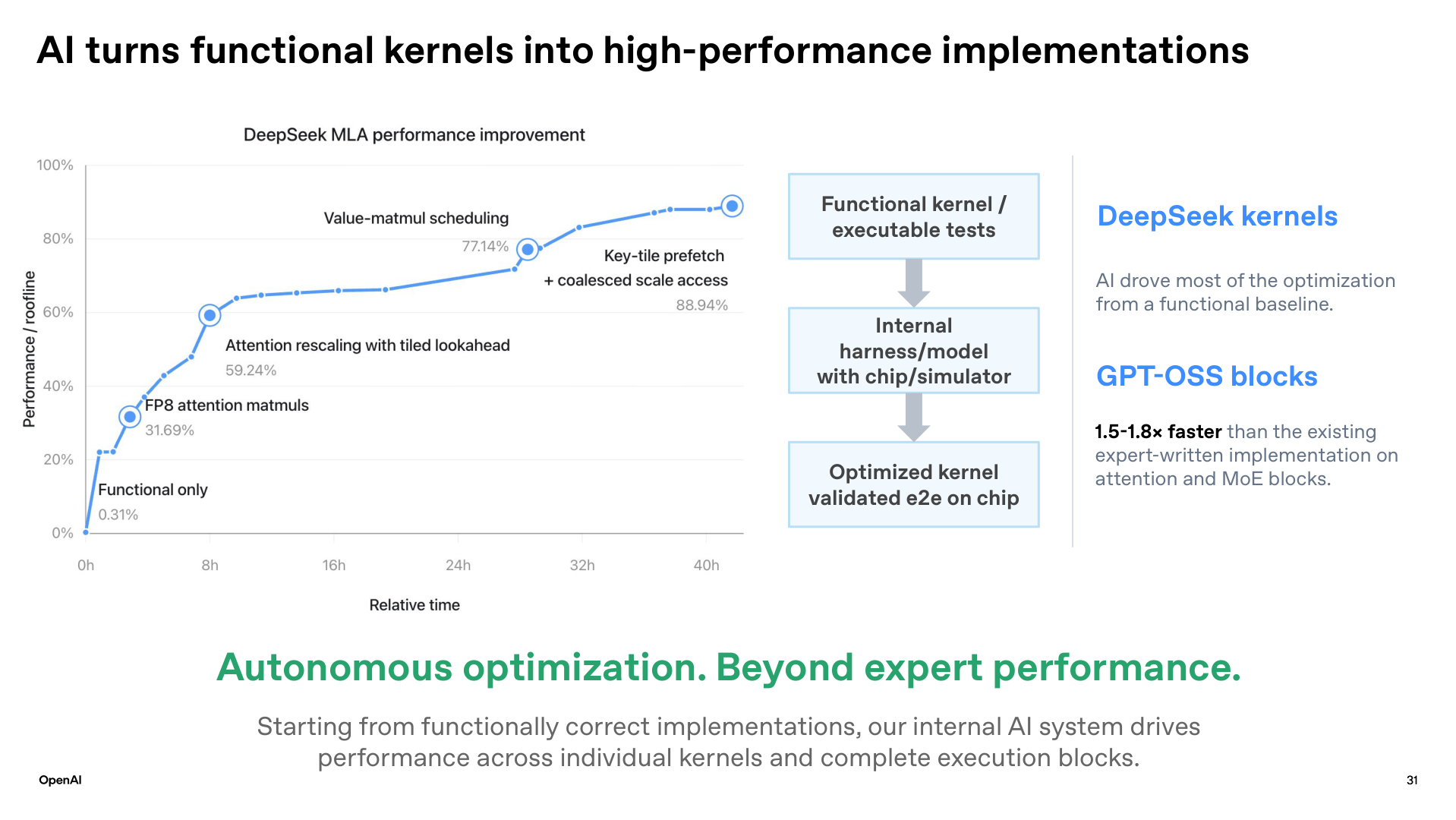
AI proposes changes to the kernel’s code. The optimization process follows this sequence:
- Start with a kernel that produces correct results.
- AI proposes a change, such as loading data earlier or changing the order of calculations.
- Tests check correctness, while measurements on a chip or simulator check speed.
- Use those results to guide further revisions, then validate the optimized kernel in the connected execution path on the chip.
The middle boxes show that checking sequence. The blue curve on the left records performance as the implementation improves.
Read the optimization steps on the graph
- The horizontal axis measures hours spent optimizing the software. Later points show progress during that process.
- The vertical axis measures achieved speed as a percentage of the estimated throughput ceiling for this calculation, called the roofline. For illustration, if the ceiling were 100 units of work per second, 89% would mean about 89 units per second. Both axes use linear scales.
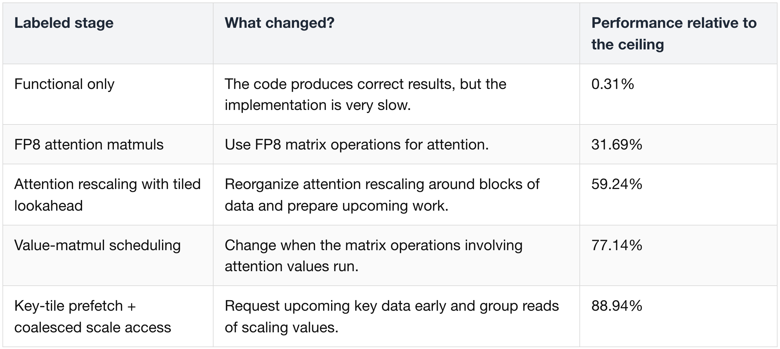
Each percentage is the resulting implementation’s performance relative to the ceiling, not an additional percentage gain. The labels summarize the changes; the slide does not provide their complete algorithms.
Connect the result to the earlier kernel-handoff example
AI can make Kernel 1 faster while creating extra work for Kernel 2. That is why its proposals must be checked across the connected execution path: the time saved must exceed any added transfer or rearrangement time, and the results must remain correct.
- The left graph demonstrates improvement in the illustrated DeepSeek attention kernel. It does not establish the same speedup for the entire model.
- The right-hand 1.5–1.8× result concerns different code and a different baseline: GPT-OSS attention and MoE blocks compared with existing expert-written implementations. It is separate from the DeepSeek graph’s improvement from a slow functional version.
6) Hardware: use AI to improve the circuits inside the chip
This subsection covers Jalapeño’s hardware: AI helps engineers explore circuit designs that perform the required calculations with less area, lower power, or better speed.
These changes happen during chip design, before manufacturing. Subsection 5 improves the code running on the chip; subsection 6 improves the circuits used to build it.
For example, a circuit multiplies two numbers. Different designs can produce the same required answer while occupying different amounts of space or taking different amounts of time. AI helps engineers propose and evaluate those alternatives.
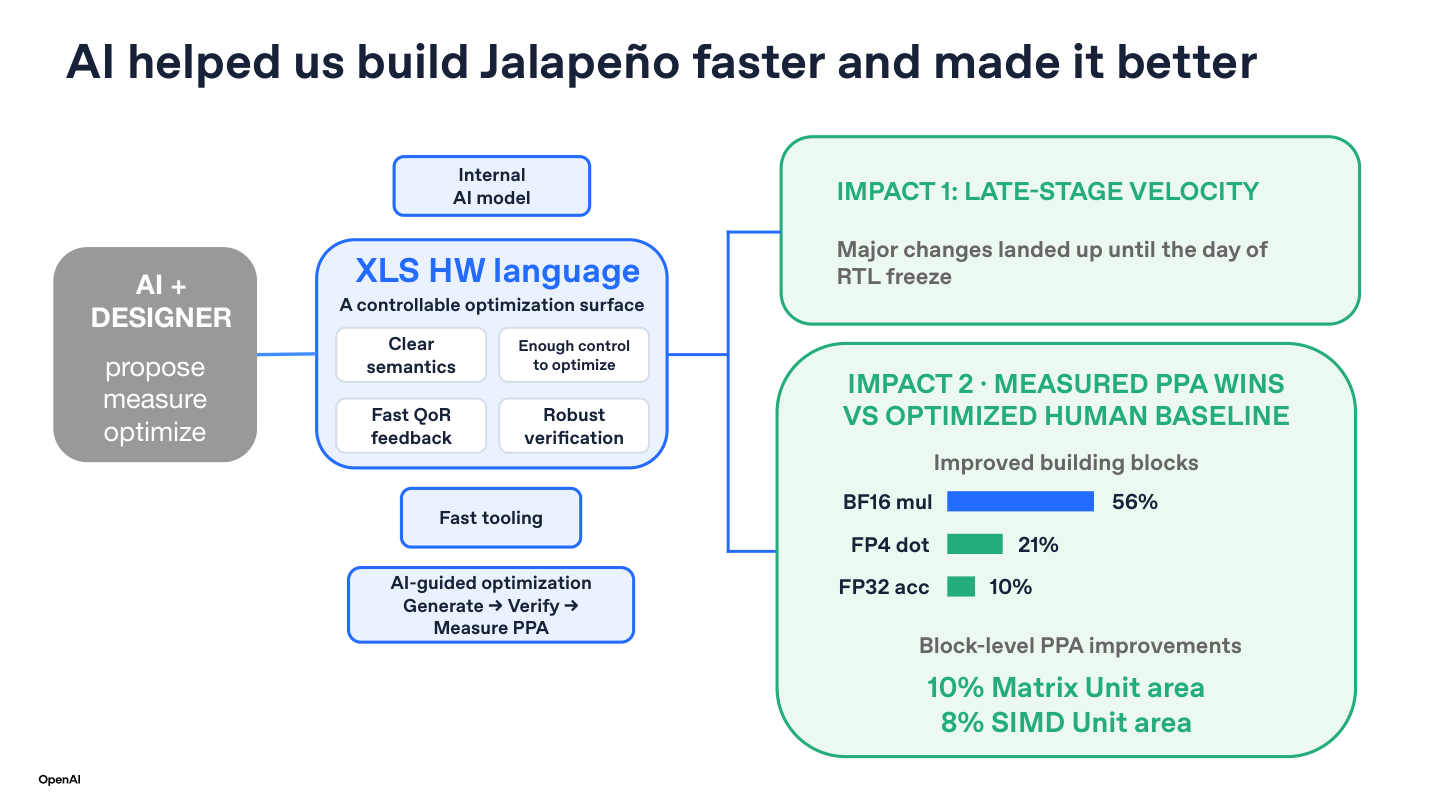
The left side shows how AI and engineers improve a circuit:
- Specify what the circuit must do. XLS, the hardware language shown in the diagram, describes the required behavior.
- Propose another implementation. AI and engineers generate a circuit design or modify an existing one.
- Verify correctness. The replacement must still perform the required calculations.
- Measure its quality. Check power consumption, operating speed and circuit area, collectively called power, performance and area (PPA). Use those results to guide the next revision.
On the right, OpenAI reports 10% less area for the matrix unit and 8% less area for the SIMD unit, compared with its optimized human-designed baseline. These savings apply to the named units. The table separates those results from the smaller building-block examples and the development claim:
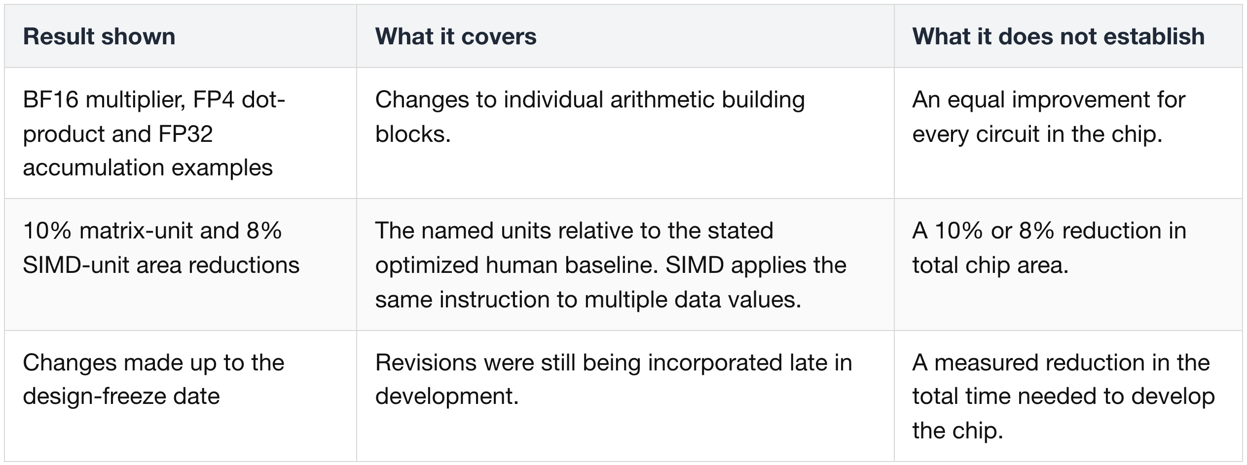
6. What these designs change in a deployed system
(1) Identify the traffic, waiting or hardware each design can remove
- The designs address different costs: moving data, waiting for results, or installing enough memory and compute. The table connects each mechanism to the condition needed for it to save time or hardware.
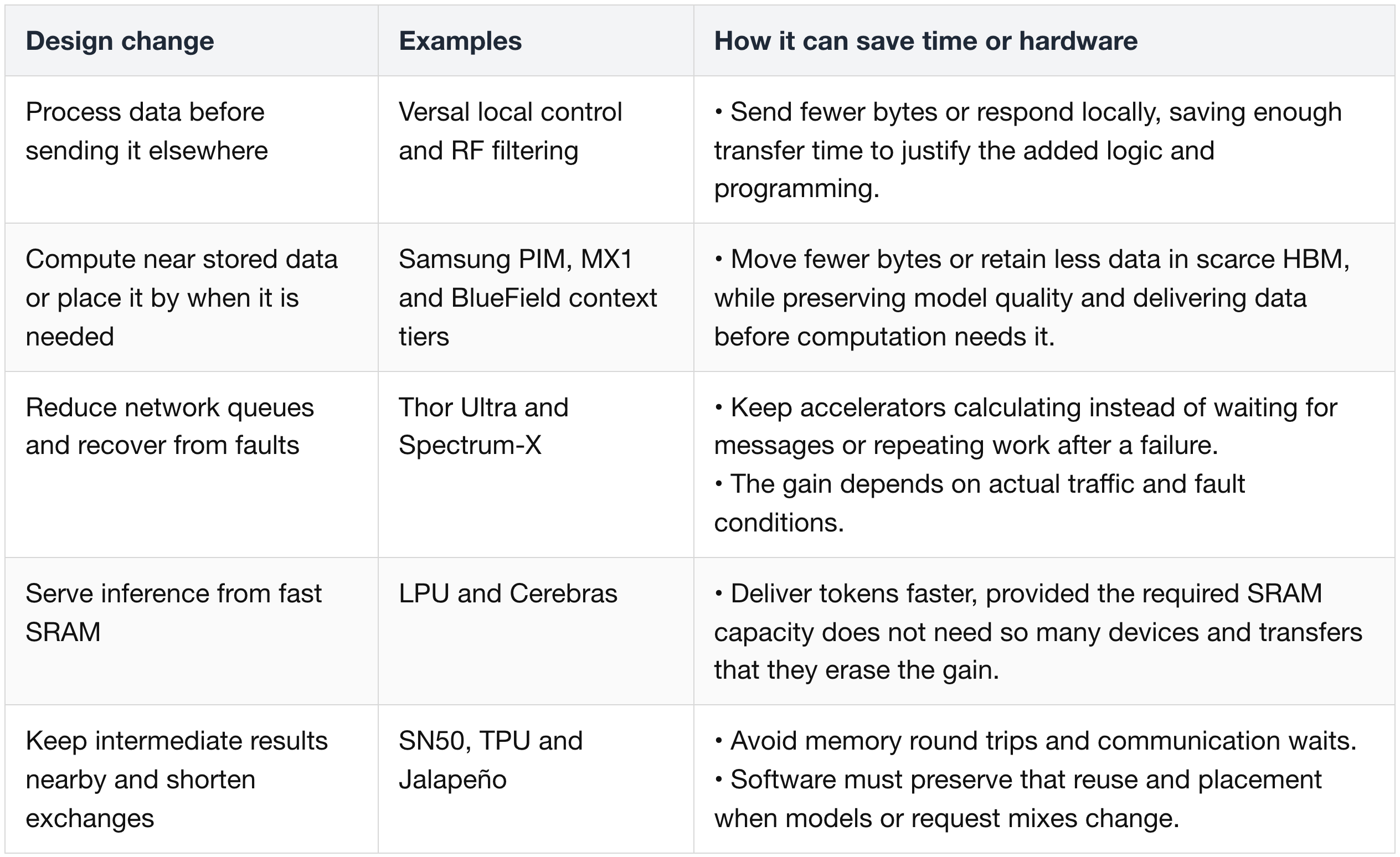
- A complete rack must supply the required compute, memory, networking, power and cooling together. A limit in one can leave capacity in another unused.