Hot Chips 2026 Tutorials | Memory

- AI infrastructure is becoming harder to improve by increasing arithmetic throughput alone.
- The memory tutorials at Hot Chips 2026 examine how capacity, bandwidth, packaging and data movement constrain AI systems.
- Memory suppliers are taking on logic, packaging, thermal design and selected computation to keep processors supplied with data.
- This article covers the six tutorial sessions on memory.
1. Memory capacity and bandwidth also depend on manufacturing
(1) Capacity, bandwidth, and latency constrain different workloads
1) Capacity, bandwidth, and request latency
- Capacity, bandwidth, and latency impose different limits:
- Capacity is how much data fits.
- Bandwidth is how much data can move per second.
- Latency is how long a particular request waits.
- Increasing one does not necessarily improve the others.
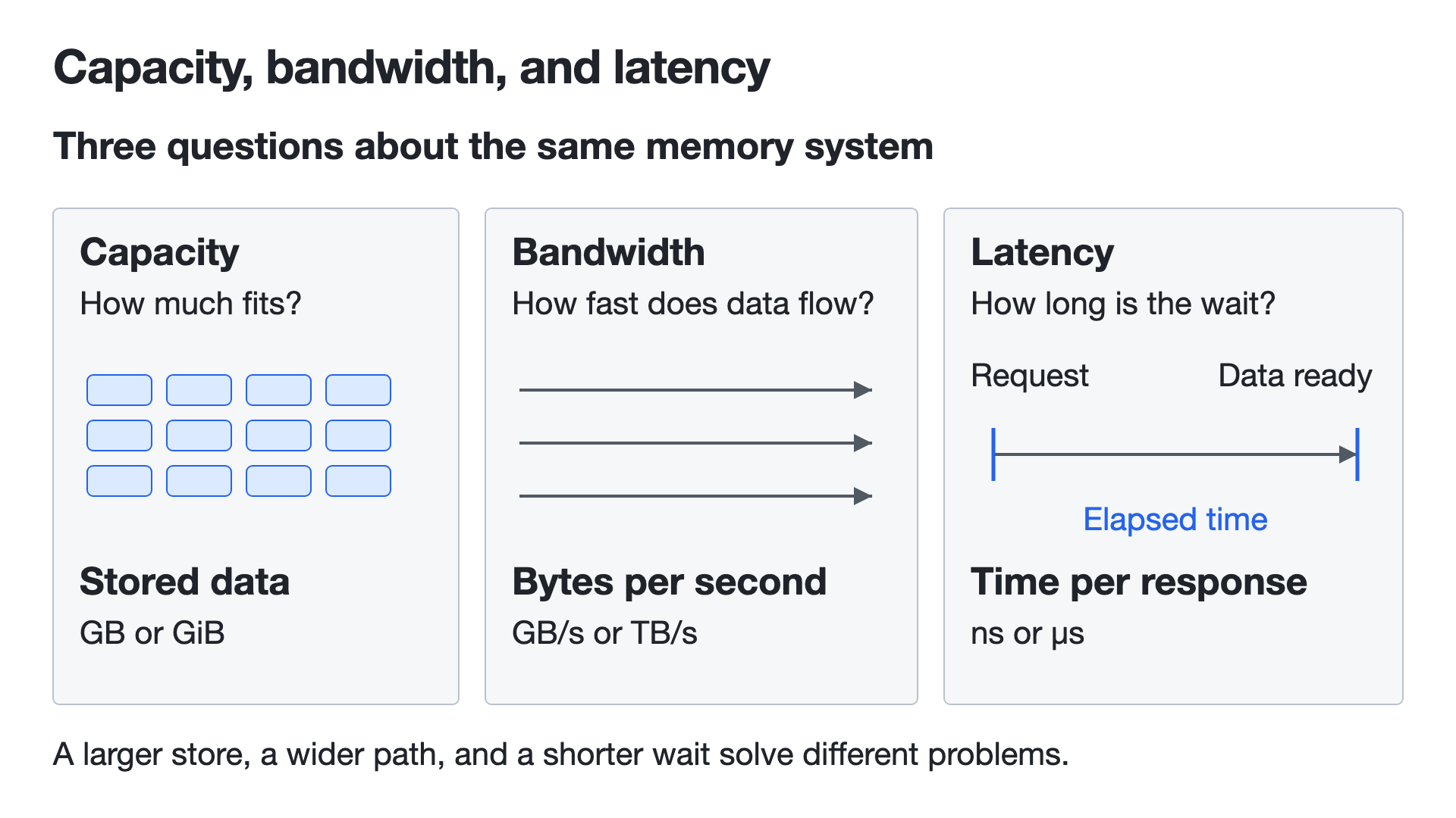
- Read the three panels as separate limits on a memory system.
- A larger store can hold more model weights or more conversation state.
- More transfer paths can supply more bytes per second.
- A shorter request path can reduce waiting on a dependent operation.
2) Prefill, decode, and stored model data
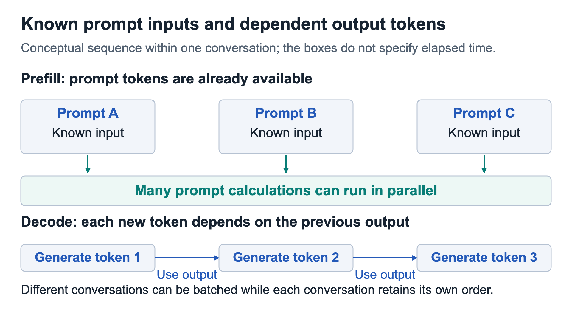
- Prefill processes the prompt before ordinary token-by-token generation begins.
- The input tokens are already known, so many of their calculations can run in parallel.
- Decode then generates the continuation. Within each conversation, the next step depends on the token produced by the previous step.
- Each decode step uses two kinds of stored data:
- Model weights are learned parameters used to produce a prediction. Conversations using the same model can share them.
- The KV cache stores attention keys and values from earlier tokens, avoiding their recomputation. Each conversation generally has its own growing cache.
- Being stored in GPU memory does not mean the data has reached the arithmetic units. Capacity determines whether it fits; reading it still takes time.
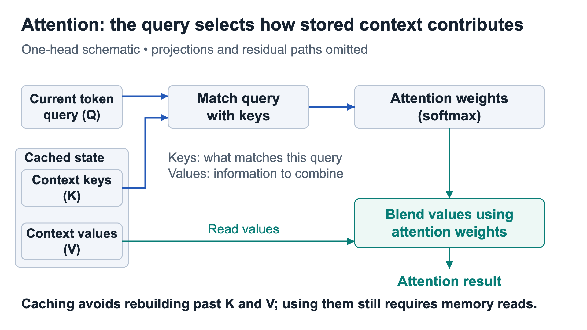
- The blue path compares the current query with stored keys and produces relevance scores.
- Softmax turns those scores into attention weights.
- The green path combines stored values using those weights to produce the result.
- The KV cache saves recomputation, but attention still has to read the context it uses.
Reuse the earlier turns of a conversation
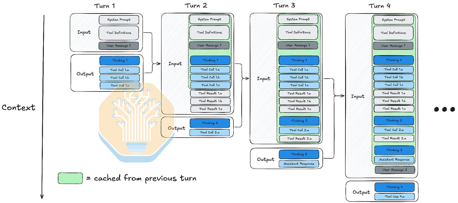
SemiAnalysis’s diagram shows one conversation growing as the AI alternates between generating text and using tools. Each column is another run of the model.
A turn here does not always mean a new user message. Receiving a tool result can also start the next turn.
Imagine asking the AI to compare two companies:
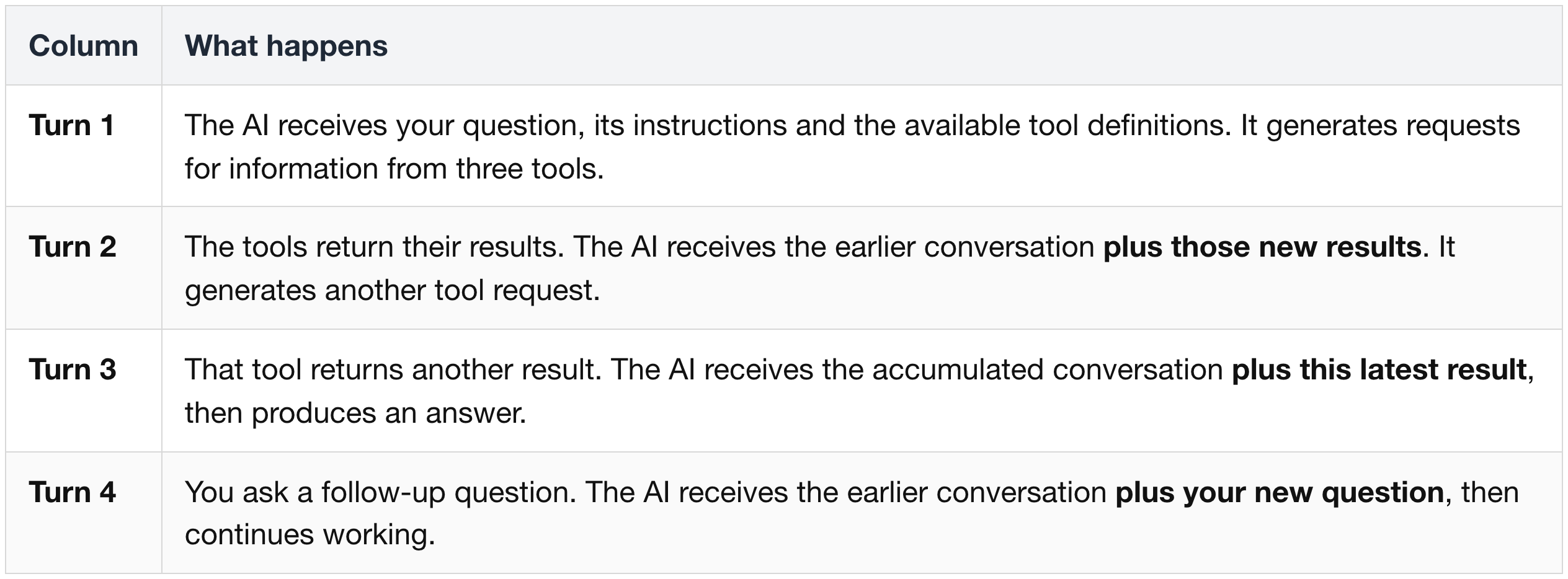
Earlier output becomes later input
The next run needs to know what has already happened: your question, which tools were requested, what they returned and what the AI answered. That history becomes part of its input.
The green areas show reusable context
The green areas indicate earlier context whose KV cache can be reused. Assuming that cache is available:
- The system retains the calculations already made for the earlier context.
- It processes the newly added messages or tool results.
- When generating its next response, it still accesses the earlier context through the cache.
Reusing earlier calculations saves processing, but retaining an increasingly long conversation still consumes memory and requires reads.
Turn 3’s green shading appears to include the newly arrived “Tool Result 2.a.” That result still needs processing when first received; the reusable portion is the context already processed.
3) Small and large decode batches
- A decode batch groups several conversations so the GPU can work on their next tokens together.
- In ordinary decoding, a batch of eight conversations can produce one next token for each conversation in the same step.
- It does not remove the sequential dependency within one conversation or produce that conversation's next eight tokens at once.
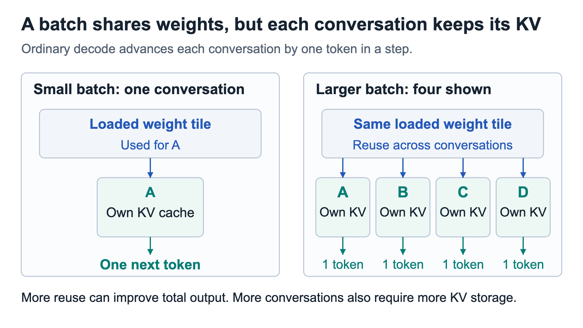
- The right panel shows four conversations reusing a loaded weight tile, with one next-token output per conversation.
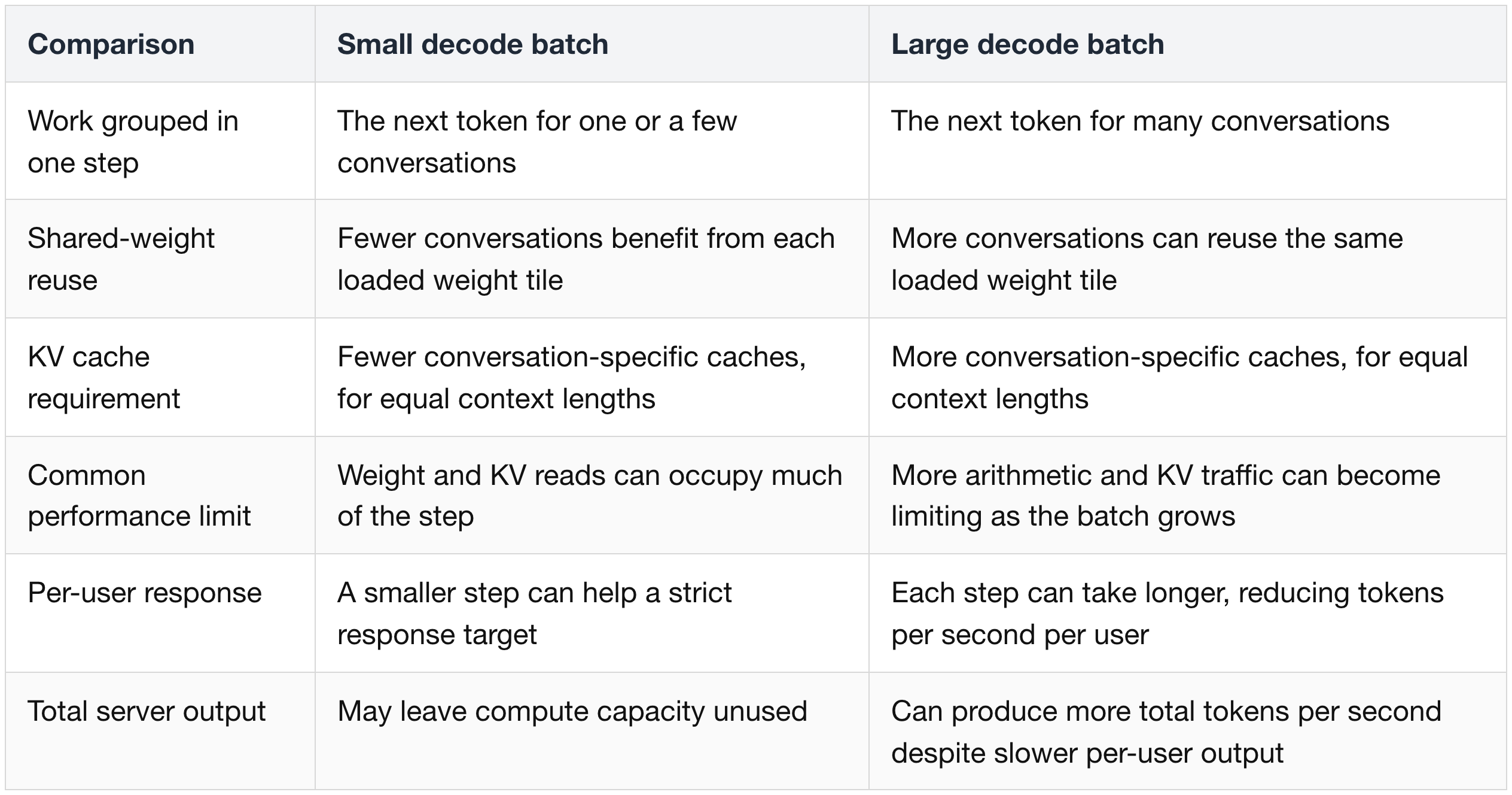
- Small batches provide fewer opportunities to reuse each weight read.
- With one conversation, a loaded weight tile contributes to one conversation's next-token calculation before the next step needs the model again.
- There may be little arithmetic to perform relative to the amount of weight and KV data that must be read. Memory bandwidth can therefore limit token-generation speed while some compute resources remain idle.
- Small batches can keep each step shorter and avoid a wait to assemble a large batch. Context length, memory traffic, and scheduling also affect per-user response time.
- Large batches reuse the shared model weights across more conversations.
- A loaded weight tile can be applied to several conversations before it is discarded, spreading the weight-reading cost over more useful arithmetic and output tokens.
- This can increase aggregate throughput, measured as tokens generated per second across all users.
- A larger step also performs more work and reads more conversation-specific KV data. The KV caches consume more memory, and per-user token generation can slow even as total output rises.
The earlier Compute Was Never the Bottleneck — Moving Bits Is article discussed why decode can be limited by weight and KV-cache delivery. The batch comparison here shows how reuse changes that demand.
4) Per-user speed versus total output
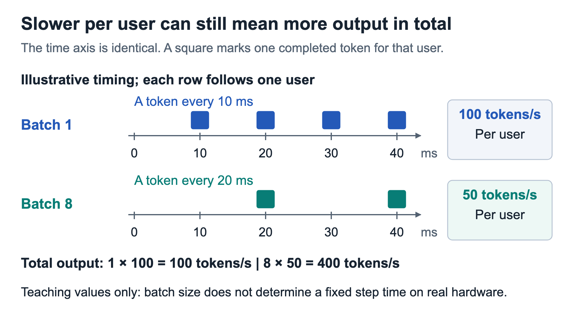
- Both rows use the same millisecond axis, and each square marks a token delivered to one user.
- An illustrative timing example separates per-user speed from total output.
- If a batch of one takes 10 ms per step, it produces 100 tokens/s for that user and 100 tokens/s in total.
- If a batch of eight takes 20 ms per step, each user receives 50 tokens/s, while the server produces
8 × 50 = 400 tokens/sin total. - The larger batch doubles the interval between tokens for each user while producing four times the total output.
5) When the workload exceeds one GPU
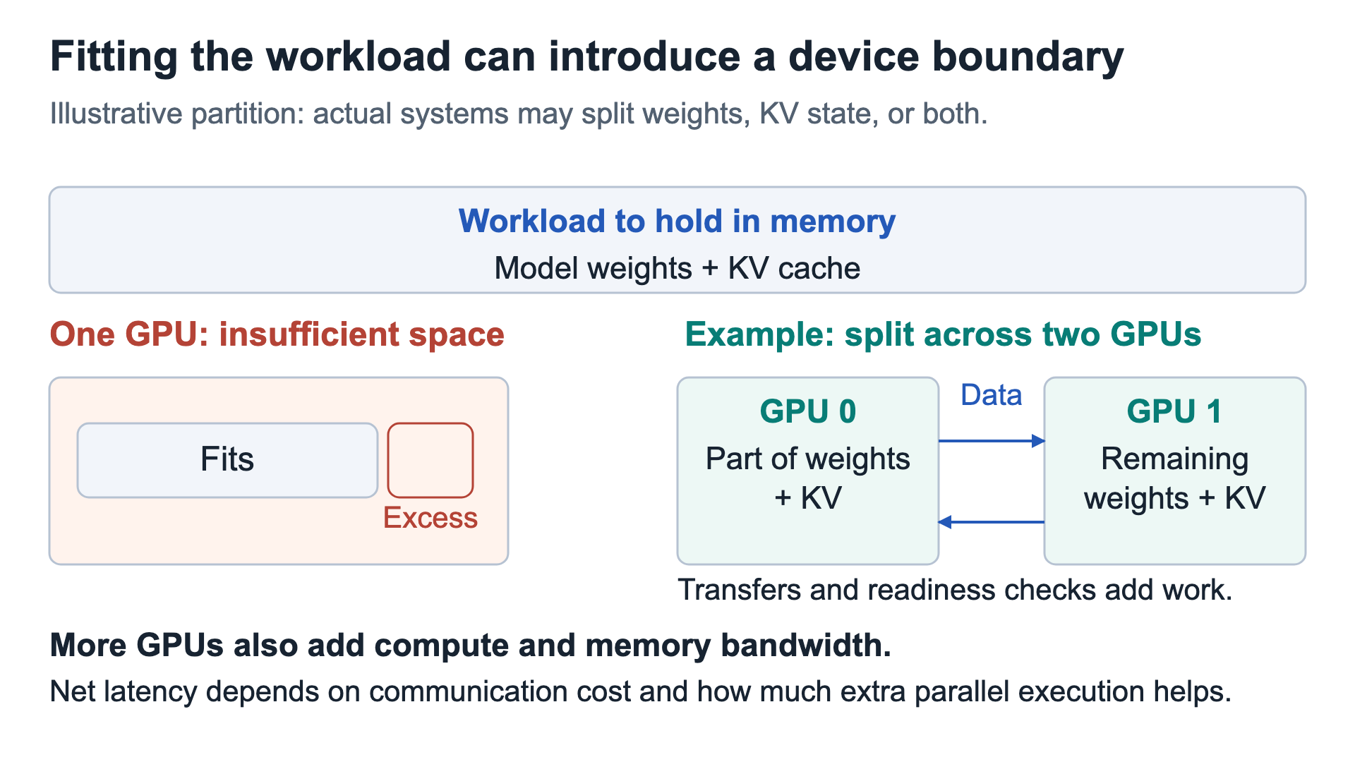
- If the model weights and KV cache exceed one GPU's memory capacity, running the workload unchanged may require distributing them across additional GPUs.
- The weights, the KV cache, or both may need to be split. This is broader than moving only the attention state.
- Depending on the partition, GPUs exchange intermediate activations, partial results, or attention data and wait for required transfers to complete.
- The resulting transfers and synchronization can add latency, depending on how much parallel execution offsets that overhead.
- A more distant network tier can add another transfer boundary if the workload extends beyond the tightly connected local group.
- However, additional GPUs also provide more compute and memory bandwidth. Since their contribution can outweigh the communication cost, using more devices does not necessarily make the request slower overall.
- More memory per GPU can sometimes let the same workload fit on fewer devices, avoiding some of those transfers and their infrastructure cost.
- Reducing batch size or context length, compressing weights or KV data, or offloading data are other ways to reduce the local capacity requirement. Each changes the workload, its representation, or the access cost.
(2) HBM consumes manufacturing resources differently
- High-Bandwidth Memory (HBM) places stacked DRAM beside the accelerator and connects them through many short data wires.
- Those wires can deliver different pieces of data in parallel, helping feed arithmetic that would otherwise wait for memory.
- The storage must also be divided into regions that can prepare those pieces concurrently. Control circuitry, vertical wiring, and stack assembly consume resources beyond the cells that actually store bits.
- In the comparison from Micron Technology (NASDAQ: MU), delivering equal HBM3E capacity consumes roughly three times as much silicon as DDR5.
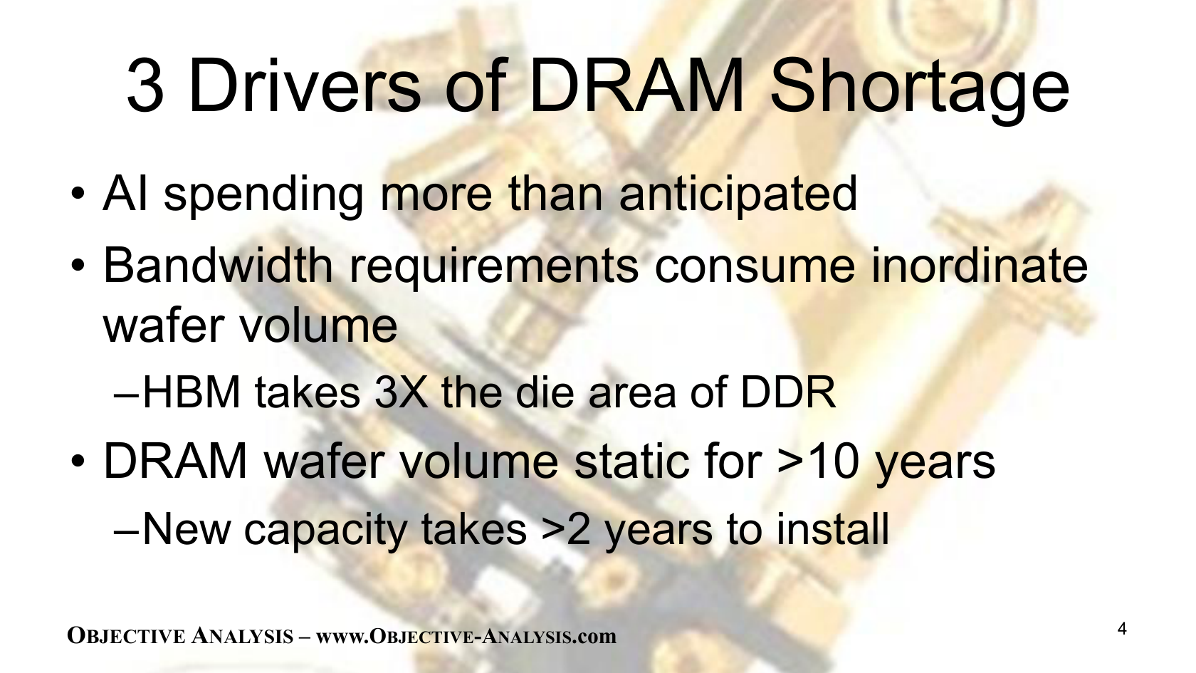
- The three listed supply pressures are: faster-than-anticipated AI demand, more wafer resources per stored bit, and slow capacity expansion.
- HBM and conventional DRAM draw on shared manufacturing capacity.
- A shift toward HBM can therefore reduce the conventional DRAM bits available from the same wafer resources.
- Adding manufacturing capacity takes years, while accelerator demand and memory mix can change more quickly.
- Micron’s June 2026 supply outlook makes that timing gap concrete:
- Management said requested HBM volumes for 2027 and 2028 exceeded its ability to supply them.
- It expected new greenfield capacity to contribute meaningfully to bit output in calendar 2028.
- It also said higher silicon use per HBM bit and new-factory costs would raise near-term DRAM bit costs.
- Announced capital spending takes time to become saleable memory; a shift toward HBM also changes how much storage existing wafer capacity can produce.
- Process improvements can fit more memory cells onto each wafer, increasing the storage produced without starting more wafers through the factory.
- Higher HBM demand can reduce the wafer capacity available for ordinary server memory.
- Delivering more HBM also requires sufficient packaging throughput and usable stacks after testing.

- The base-die and custom-memory options aim to perform selected operations where the data is stored, reducing transfers to the main processor.
- The final software-support item is a practical constraint: moving arithmetic into memory helps only when the compiler and runtime can place suitable work there.
2. Micron: more parallel paths create bandwidth, with physical costs
(1) Follow the hierarchy from cells to data paths
1) Cells, banks, and the controller
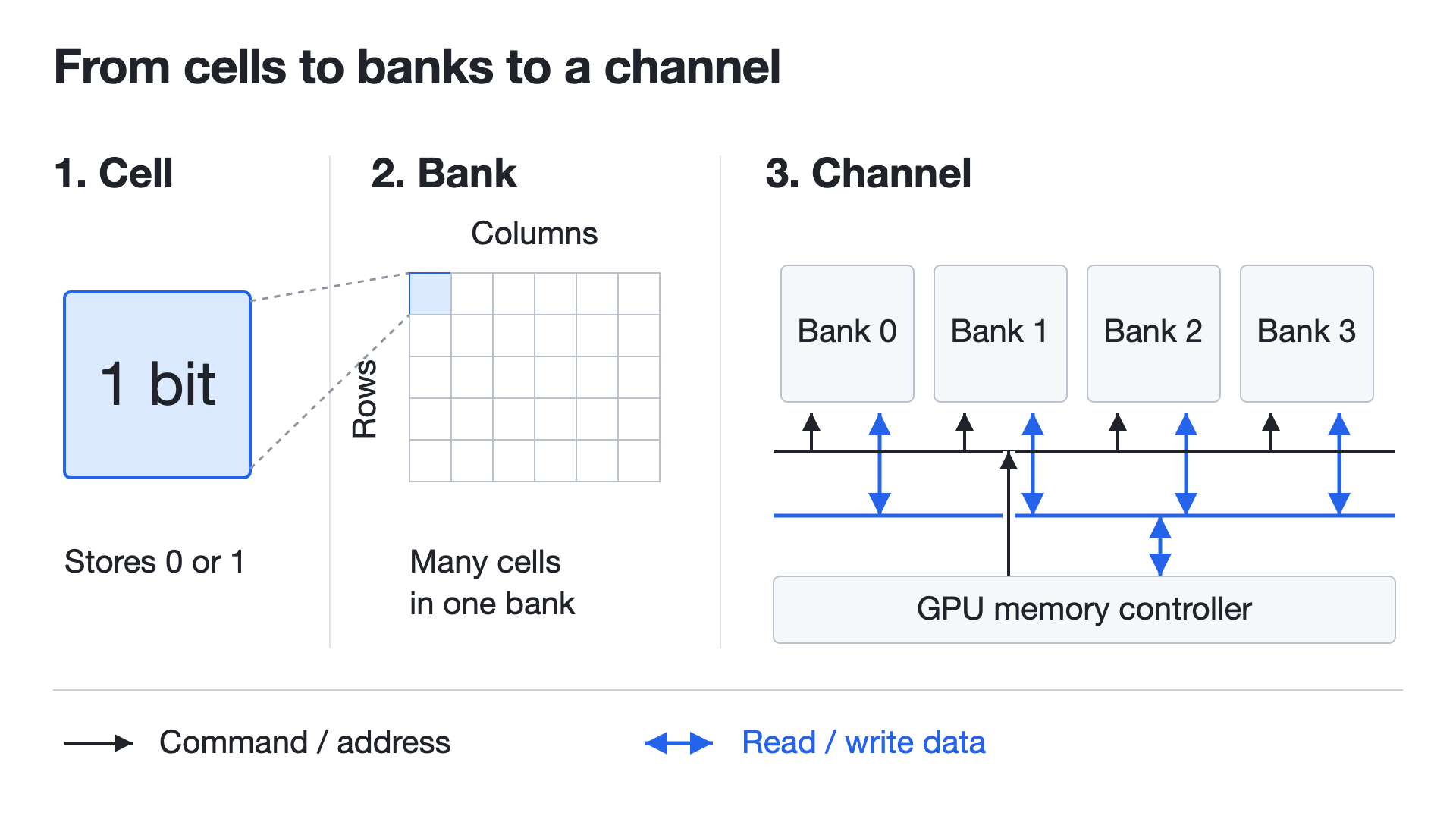
- A DRAM cell stores one bit.
- Banks group many cells into storage regions that can prepare different requests with some independence.
- Reading a bank involves internal operations that take time. While one bank is occupied, another eligible bank can prepare data for a different request.
- The memory controller schedules these operations, deciding which request can proceed without violating the memory's timing rules.
2) Channels and pseudo-channels
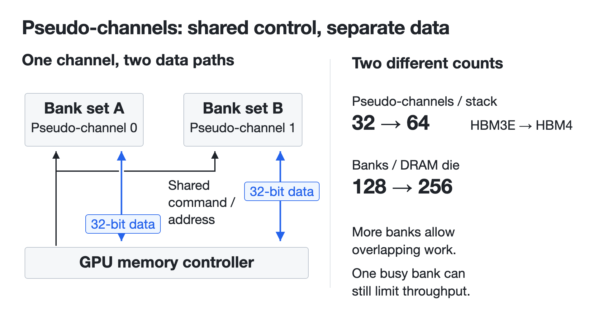
- A channel connects that controller to a set of banks through two kinds of wiring.
- Command / address wires specify the operation and the location to access, such as reading a particular bank and address.
- Data wires carry the actual stored values, such as model weights, back to the GPU or carry new values into memory.
- In Micron's description, each channel has two pseudo-channels: separately usable data paths to their banks that share command / address resources.
- Sharing instructions does not force the two paths to share one data bus. Eligible transfers can use separate buses, although their commands still have to be scheduled through the shared resources.
3) What HBM4 doubles
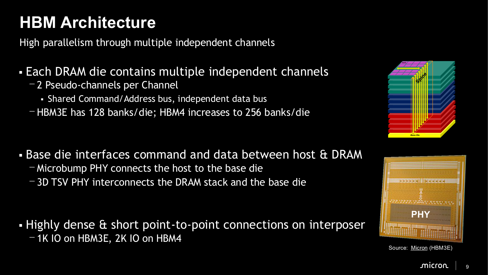
- The yellow connections carry signals vertically between storage layers and the base die.
- The base die connects the stack to the GPU.
- A read request needs a scheduled route to the stored cells, then a data path back to the GPU.
- Stacking adds storage above that interface.
4) When more banks help
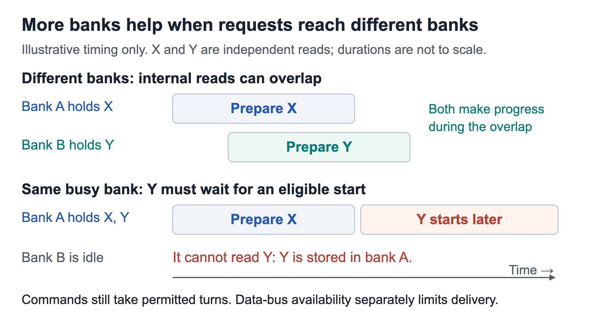
- Suppose the GPU needs two groups of model weights, X and Y, and already knows where both are stored.
- These are independent reads: the GPU can request Y without first receiving X. The memory system has two requests it can try to make progress on.
- First, suppose X is stored in bank A and Y in bank B.
- Bank A starts the internal work needed to read X. Before that work finishes, the controller can start bank B's read of Y, provided the timing rules allow it.
- The two banks can therefore spend part of the same interval preparing their data. Reading Y does not have to wait for all of bank A's work on X to finish.
- Once ready, the data travels to the GPU over the available data buses. Whether the transfers themselves can overlap also depends on which buses the banks use.
- Now suppose both X and Y are stored in bank A, and bank A is performing an internal operation that prevents it from starting the next requested read yet.
- That next read has to wait. Bank B may be idle, but it cannot supply Y because Y is stored in bank A.
- Banks are different storage locations, not interchangeable workers that can retrieve any data. The address of the requested data determines which bank must serve the read.
- Shared command wiring adds a separate scheduling limit.
- The controller sends instructions such as which bank and address to read. Requests using the same command wires must take their permitted turns on those wires, even when the banks can overlap their internal work afterward.
- More banks help when several pending requests target different banks that are ready to work. More data buses help carry the resulting data. Neither change guarantees that one particular read will finish sooner.
- The bank count is therefore not another multiplier to apply to the interface bandwidth. Banks help sustain the stream of data. The width and speed of the data wires set its external transfer ceiling.
5) Why each burst remains 32 bytes
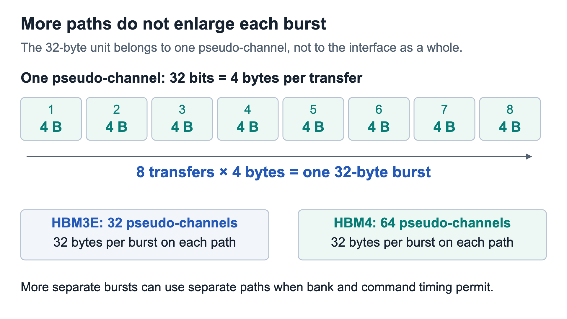
- A burst is a short sequence of transfers, rather than one individual transfer.
- One transfer: 32 bits = 4 bytes on one pseudo-channel.
- One burst: 8 successive transfers × 4 bytes = 32 bytes.
- Burst length counts the transfers (eight here). Burst size counts the total bytes delivered (32 here).
- The 32-byte access unit describes one burst on one pseudo-channel, rather than the amount carried by all pseudo-channels together.
- HBM3E has 32 such data paths, while HBM4 has 64. Each path still carries 32 bytes per burst, so the wider overall interface can serve more separate bursts without making an individual burst larger.
- Suppose a workload needs many separate 32-byte pieces of data.
- Each piece fits in one burst. Additional pseudo-channels let more of those reads use separate data paths, when the banks and command timing allow it.
- The benefit comes from handling more pieces in parallel. The workload does not have to request a 64-byte piece just because the total interface width doubled.
6) When transferred bytes go unused
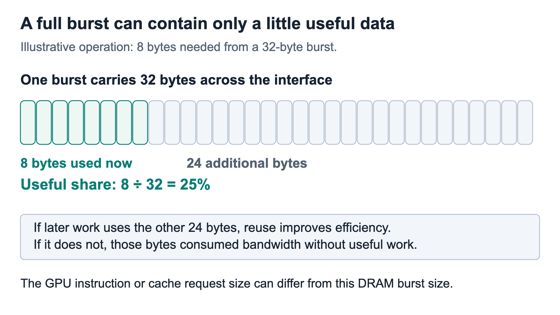
- Now suppose an operation needs only 8 bytes from a region fetched in one 32-byte burst.
- The burst still carries 32 bytes: the 8 bytes needed by that operation and 24 additional bytes.
- If no later operation uses those additional bytes, only 8 of the 32 transferred bytes, or 25%, contribute useful data. They still all consume transfer capacity.
- More pseudo-channels can carry more bursts, but they do not shrink each burst to the 8 bytes this operation needs. Reusing the additional bytes can improve efficiency without changing the burst size.
- HBM4 adds parallel transfer capacity while preserving the same transfer granularity.
- Whether that capacity carries useful data still depends on the workload's access pattern and reuse.
- These examples describe the DRAM interface's burst size. A GPU instruction or cache request can involve a different amount of data, potentially requiring several bursts.
(2) Wider interfaces raise bandwidth, but useful delivery depends on the workload
1) Combine more data paths with faster signaling
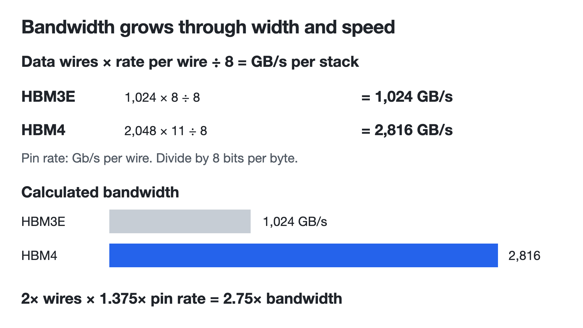
- The diagram separates the two multipliers.
- Data I/O doubles from 1,024 to 2,048 bits.
- The nominal rate per wire rises from 8 to 11 Gb/s.
- Together, twice the interface width and faster signaling provide approximately 2.75 times the nominal bandwidth: about 2.8 TB/s per stack in Micron's comparison. Both changes contribute to the increase.
- Adding storage layers increases capacity, but does not widen the external interface in the same proportion. A taller stack can hold a larger model without delivering each repeatedly read weight faster.
2) Why useful bandwidth falls below the ceiling
- The nominal bandwidth is a ceiling, assuming the wires keep carrying useful data at their stated rate.
- Refresh periodically maintains the stored DRAM data and consumes memory-operation time.
- Bank conflicts make requests wait for an occupied storage region. Command timing limits when the next operation can start.
- An access can also fetch bytes the calculation does not use. Those bytes occupy the interface without contributing useful work.
- The GPU therefore needs both enough independent requests to keep the paths active and enough reuse or useful bytes in each transfer.
3) Silicon cost and access-pattern efficiency
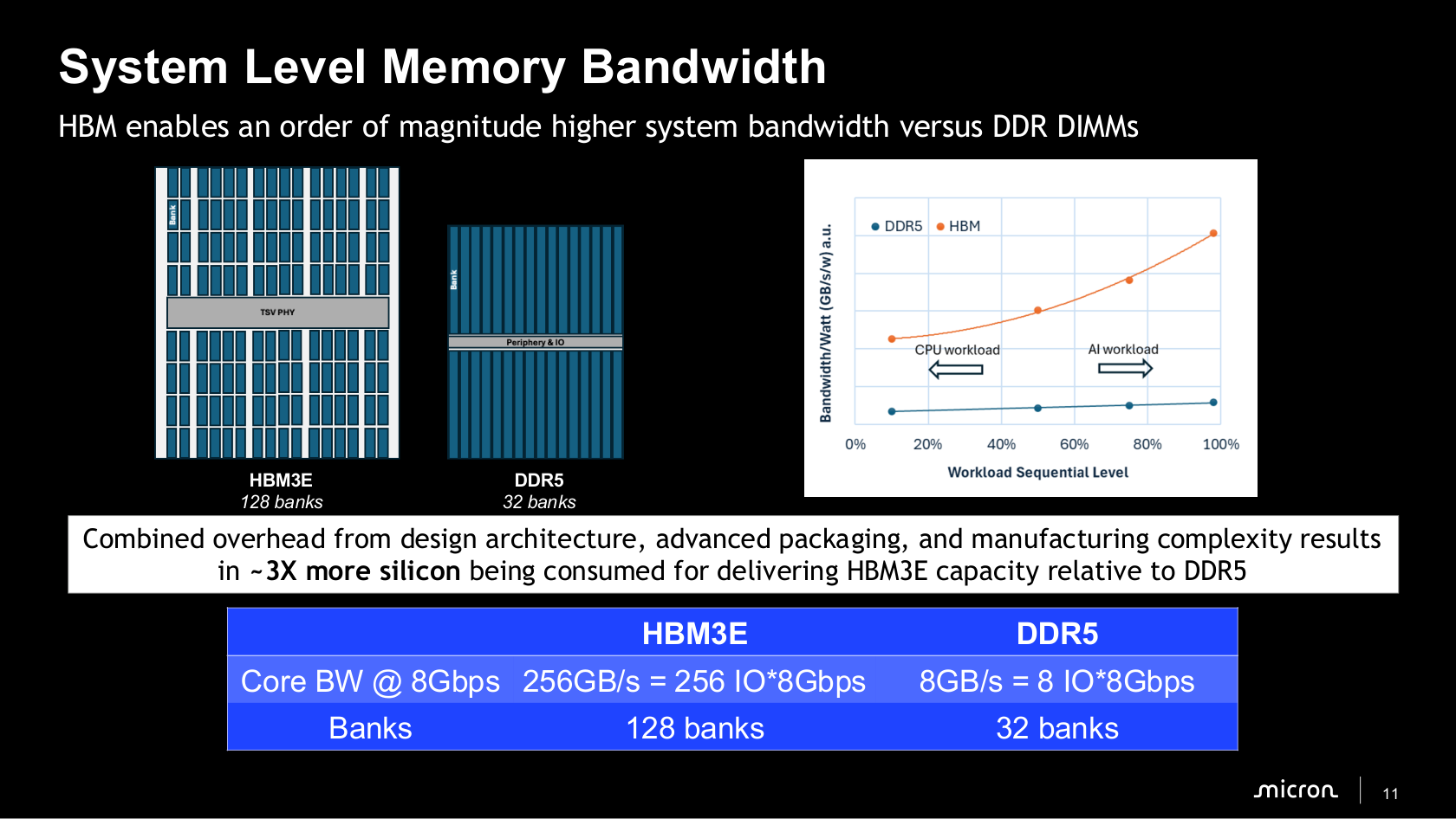
- The left floorplans show the physical cost of preparing many requests in parallel: HBM3E divides storage into 128 banks, compared with 32 in the illustrated DDR5 die, and devotes space to vertical-interface circuitry.
- The roughly 3× silicon-consumption statement covers the combined architecture, packaging, and manufacturing overhead for equal HBM3E capacity. It cannot be attributed to bank count alone.
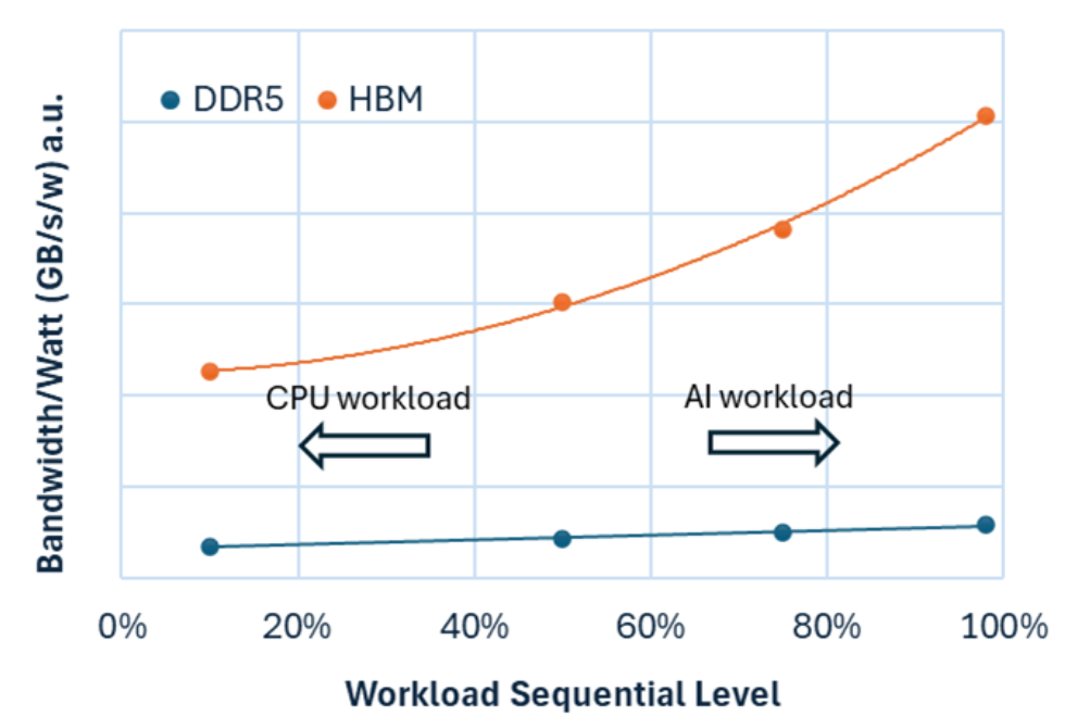
- Read the axes and the two curves together.
- The horizontal axis runs from 0% to 100% workload sequentiality. Moving right means reading data in more continuous sequences of memory locations.
- Sequentiality here refers to the memory locations being accessed, not to generating output tokens sequentially.
- The vertical axis is bandwidth per watt: how much data is delivered per second for each watt consumed. Equivalently, it describes data delivered per unit of energy.
- The orange HBM curve rises substantially as accesses become more sequential, while the blue DDR5 curve rises only slightly. HBM therefore shows a larger energy-efficiency advantage for the more sequential workloads in this comparison.
- A sustained stream means that the controller has a continuing supply of memory requests it can schedule.
- Suppose the GPU needs a large group of model weights stored in consecutive locations and already knows which blocks it needs.
- It can request upcoming blocks without waiting for each preceding block to arrive. These reads give the controller several opportunities to make progress.
- When the banks and data paths are available, HBM can keep delivering successive bursts with fewer gaps.
- A dependent lookup behaves differently.
- First, the GPU reads X. It then uses the value of X to determine where Y is stored, and only then can it request Y.
- Additional data paths cannot accelerate that lookup while the system does not yet know what to request next.
- Other independent work could still use those paths. The dependency limits this chain of reads, rather than necessarily leaving the entire memory system idle.
- These examples illustrate how an access pattern can affect delivery. The graph shows the relationship between sequentiality and bandwidth per watt, but does not separately quantify which scheduling or internal-memory effects produce the curves.
- HBM is itself a type of DRAM. Here, the desired-memory column compares HBM with conventional DDR5 DRAM. The choices are conditional workload fits, and the processor and package must support the chosen memory type.
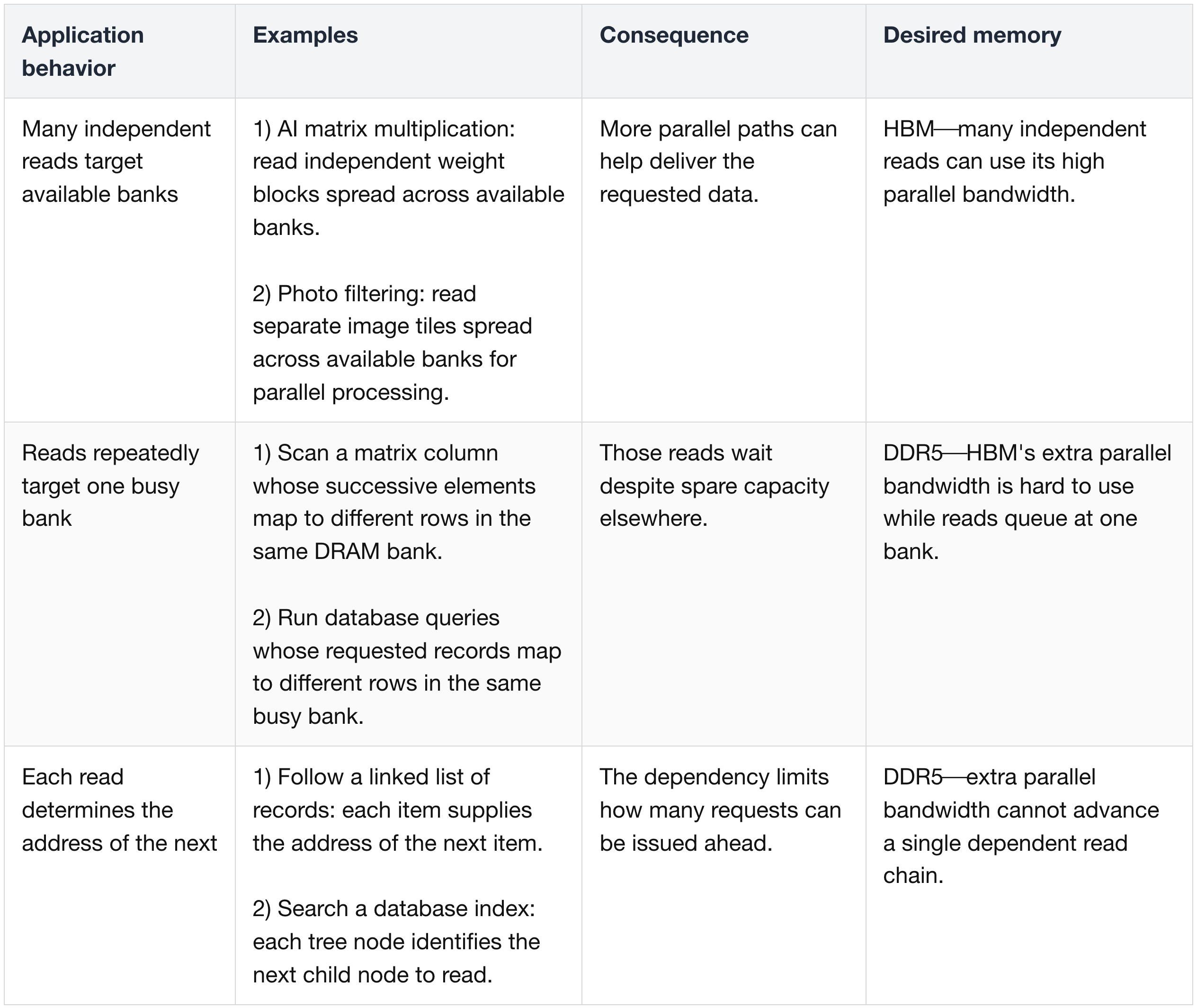
- These examples assume the reads reach DRAM. Cache hits, physical address mapping, and request scheduling can change which limitation the application encounters.
- For a single dependent lookup chain, compare measured access latency. The table does not claim that DDR5 has lower latency than HBM, and HBM can be useful for other requirements even when its extra bandwidth does not accelerate that chain.
- Scattered addresses alone do not imply poor utilization.
- Many independent, scattered reads can still use different banks effectively.
- The important questions are whether enough requests are ready, whether their banks can serve them, and whether the application uses the bytes transferred.
(3) Electrical, thermal, and data-integrity challenges
1) Electrical and thermal costs
- Faster signaling reduces the time available to identify each bit correctly.
- The receiver must distinguish the intended bit within a shorter interval, making reliable transmission more demanding.
- This is a harder design requirement, rather than a claim that every faster interface produces more errors. A properly designed faster interface can still meet its required reliability target.
- More banks and connections consume silicon.
- Faster interfaces and more base-die logic generate heat.
- A taller stack also makes it harder for heat near the bottom to reach the cooler above it.
- Electrical, thermal, and mechanical design consequently become part of the memory performance problem.
2) What ECC and CRC protect
- Faster signaling gives the receiver less time to identify each transmitted bit correctly.
- Physical interface design must keep the signal reliable within that interval.
- If a covered error still occurs, ECC or CRC can detect it; a suitable ECC can also correct it.
- These checks also protect stored or transferred data at lower speeds. Higher speed adds a design challenge, but error protection is useful at any speed.
- Error protection helps the GPU distinguish the intended data from a value changed by a storage or transmission fault.
- A damaged bit can turn one valid number into another. As an example,
00001101represents 13, while changing one bit to produce00001001changes the value to 9. - Without check information, the GPU may accept 9 and continue with an incorrect weight or intermediate result. An error that escapes detection is called silent data corruption.
- A damaged bit can turn one valid number into another. As an example,
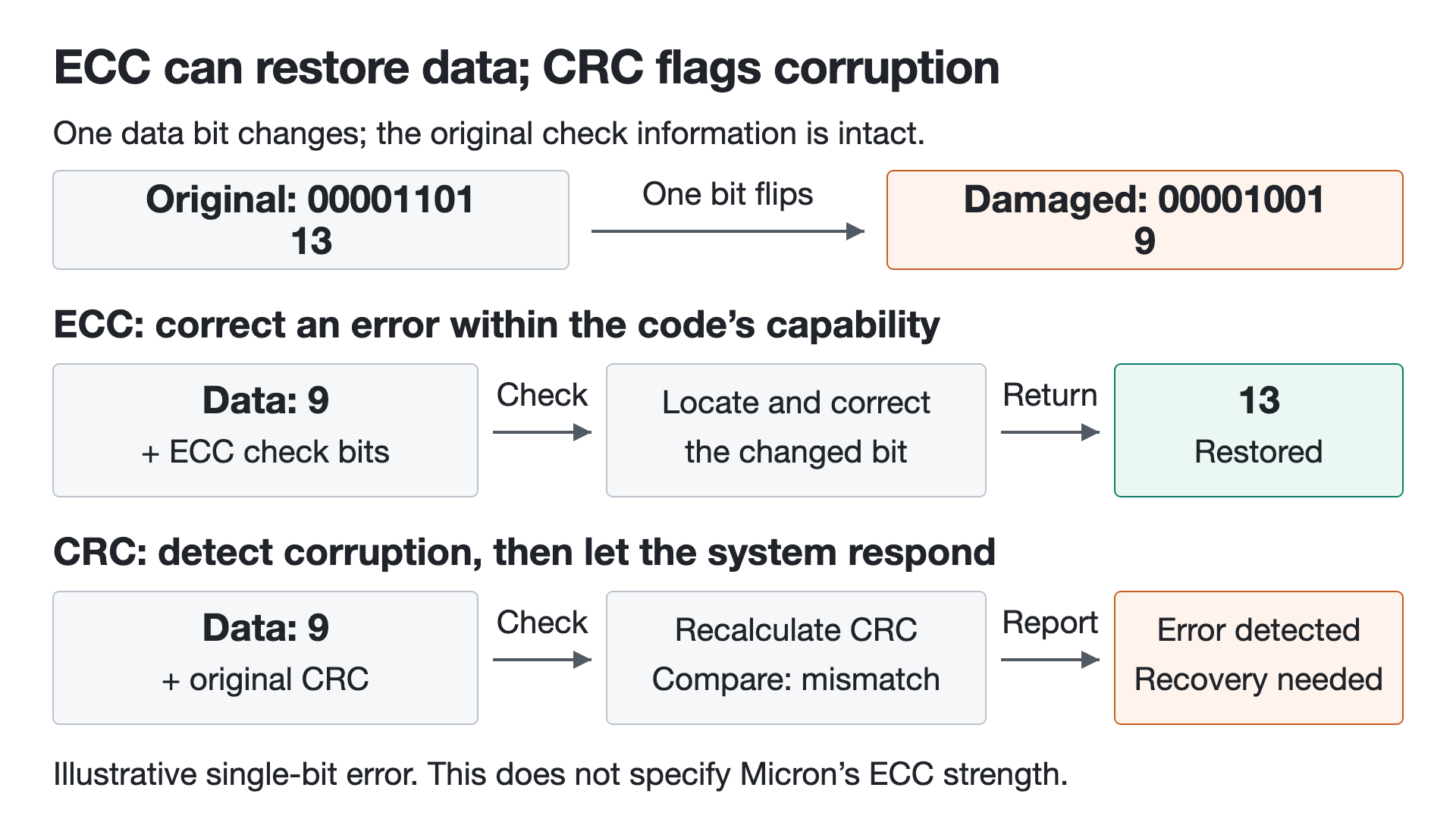
- The same single-bit error enters both paths: the ECC example reconstructs 13, while the CRC path reports the mismatch for a separate recovery action.
- An error-correcting code (ECC) works in three steps:
- Calculate redundant check information from the original data and store it alongside the data.
- On a read, test whether the data still satisfies those encoded relationships.
- For an error pattern the code can correct, use the failed checks to reconstruct the intended value.
- A suitable single-bit-correcting code could restore 13 in this example. It needs neither a full duplicate of the data nor a physically repaired cell.
- A cyclic redundancy check (CRC) tests whether a transfer matches its check value:
- The sender calculates a check value from the data.
- The receiver calculates it again from the received data.
- A mismatch signals that the transfer failed the check.
- The CRC does not reconstruct the original value. Recovery needs a separate action, such as another transfer where supported.
- A matching check means no error was detected; some error patterns can still escape detection.
3) On-die and system-level coverage
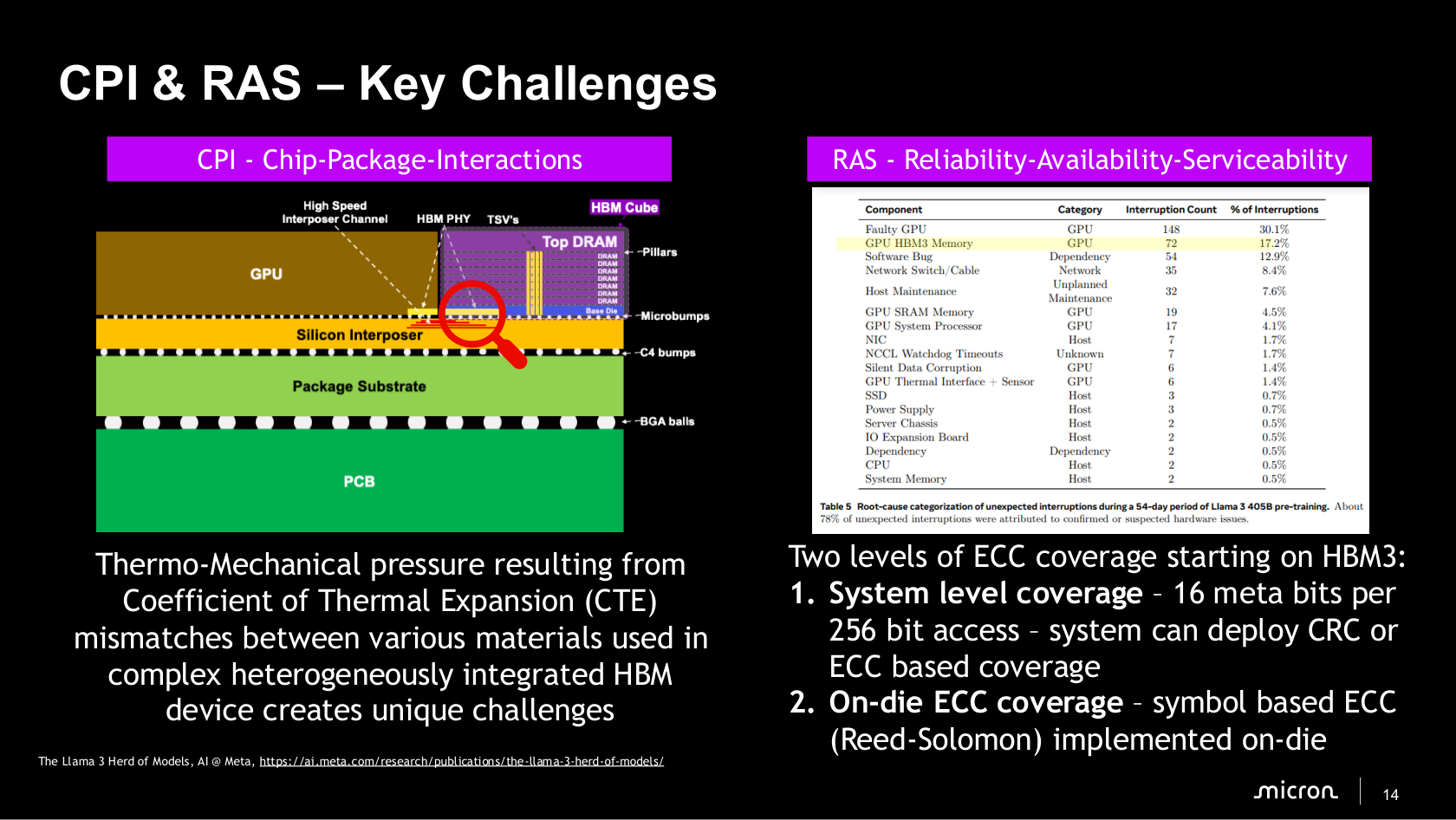
- The lower-right protection items answer where an error can be caught along the data's journey.
- Data is checked inside the DRAM die by on-die protection.
- It then travels through further circuitry and connections toward the GPU.
- A new error introduced after the on-die check is outside that check's coverage. Protection spanning the relevant later path is needed to detect or correct covered errors introduced there.
- The design provides two levels of protection:
- On-die Reed–Solomon ECC covers errors within the die.
- A wider system provision allocates 16 metadata bits for every 256 data bits.
- It is space for a system-selected checking scheme, not an ability to correct 16 damaged bits.
- Higher signaling rates make reliable delivery across those later interfaces more demanding, connecting this coverage question to the speed discussion above.
- The need for different protection boundaries also exists at lower speeds. It depends on where a fault can occur and where the data is checked, rather than on speed alone.
- Memory faults can interrupt jobs or produce incorrect results even when the memory interface has a higher nominal transfer rate.
3. Samsung, SK hynix, and d-Matrix move the boundary between memory and compute
(1) Samsung: turn the HBM base die into a logic platform
Samsung Electronics (KRX: 005930) proposes three stages:
- a) reclaim processor area,
- b) add functions to the base die,
- c) then place memory vertically above the processor.
- The DRAM core dies store data. The base die beneath them provides communication and control circuitry.
- An advanced logic process gives the base die room for more capable circuitry, while the storage stack keeps a process suited to dense DRAM cells.
- These phases are an architectural roadmap, not features all established in mass production.
- By Q2 2026, Samsung had reached a nearer-term commercial step: expanding HBM4 sales and supplying HBM4E samples to major customers. Those milestones do not establish that the later compute-in-base-die or zHBM concepts are shipping.
1) Phase 1: reclaim processor area and manage the relocated circuitry
Relocate the controller
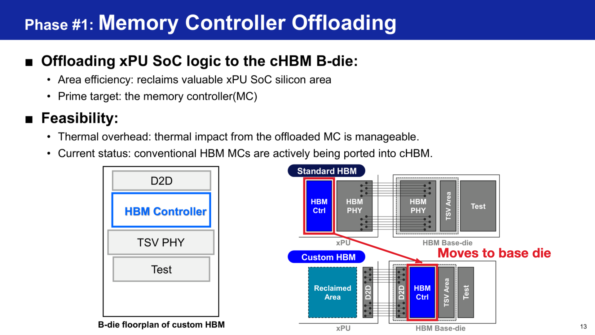
- The HBM controller turns processor requests into reads, writes, and refresh operations that respect DRAM timing and bank availability.
- In the upper standard-HBM diagram, the controller occupies area in the xPU, meaning the CPU, GPU, or other processor using the memory.
- In the lower custom-HBM diagram, it moves into the HBM base die. The red rectangles mark the relocation, and a die-to-die connection carries requests between the xPU and the controller.
- The reclaimed area (teal) becomes available for other processor functions. The GPU's main computation remains on the GPU.
- Phase 1 also replaces the conventional HBM electrical interface with a smaller die-to-die interface. Together, interface shrinkage and controller relocation free processor area.
- The controller still consumes silicon and power in its new location. The processor and memory supplier must agree on the request interface and validate the design together, so reclaimed xPU area does not by itself establish a lower total system cost.
Replace defective storage
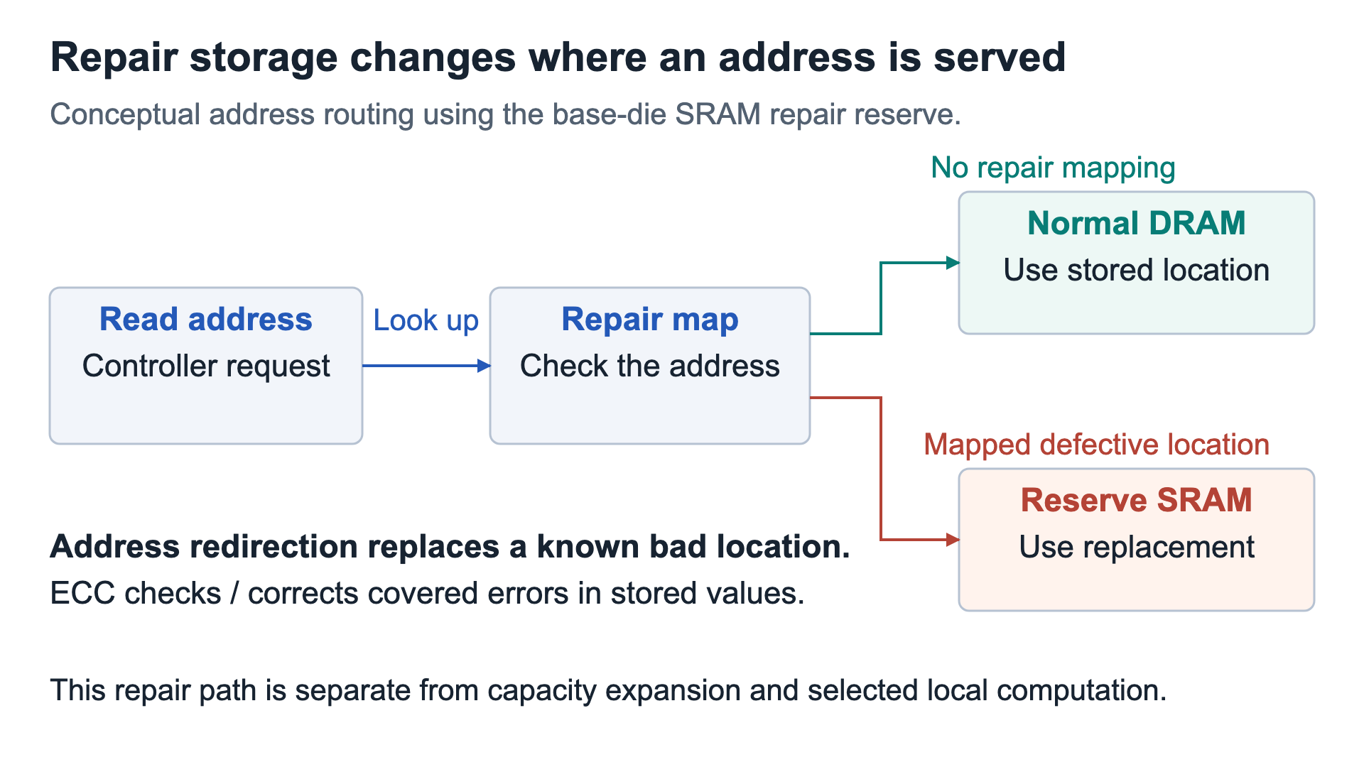
- The base die holds a small reserve of SRAM, a type of working memory implemented differently from DRAM.
- Suppose address A belongs to a known defective DRAM location:
- A repair map assigns A to a working SRAM slot.
- The GPU continues to request address A.
- The controller redirects that request to the SRAM slot.
- Unmapped addresses still use normal DRAM, as shown in the other path.
- This avoids the faulty location without physically fixing it or recovering already-lost data by itself. ECC instead uses extra checking information to detect and, within its capabilities, correct corrupted values.
Remove concentrated heat
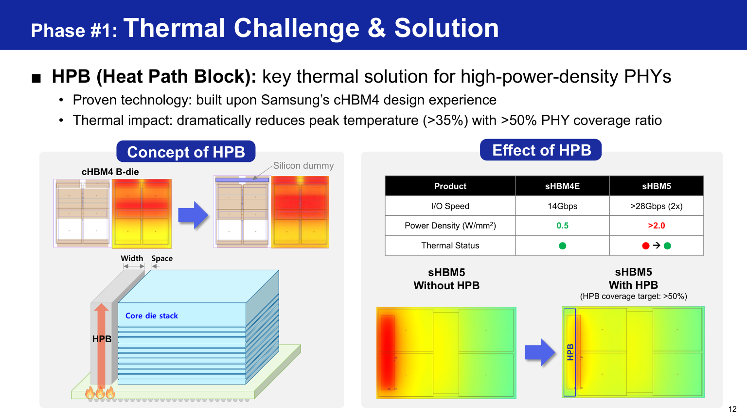
- A smaller interface concentrates its power in less area. Even if each transferred bit requires less energy, faster traffic can raise total power and create a hot spot beneath the DRAM stack.
- The lower-left upward arrow shows a Heat Path Block (HPB): a dummy silicon structure beside the storage dies that gives heat an additional route upward from the interface.
- The lower-right maps compare the design without and with that path. The previously red hot region becomes cooler yellow / green.
- Samsung reports a peak-temperature reduction above 35% with more than 50% interface coverage under its stated conditions.
- The slide does not provide the absolute temperature baseline needed to translate that percentage into degrees Celsius.
2) Phase 2: add monitoring, memory expansion, and local computation
- With the controller on the base die, remaining space can accommodate additional functions. These are separate design choices with different benefits and costs.
Monitor and test the stack
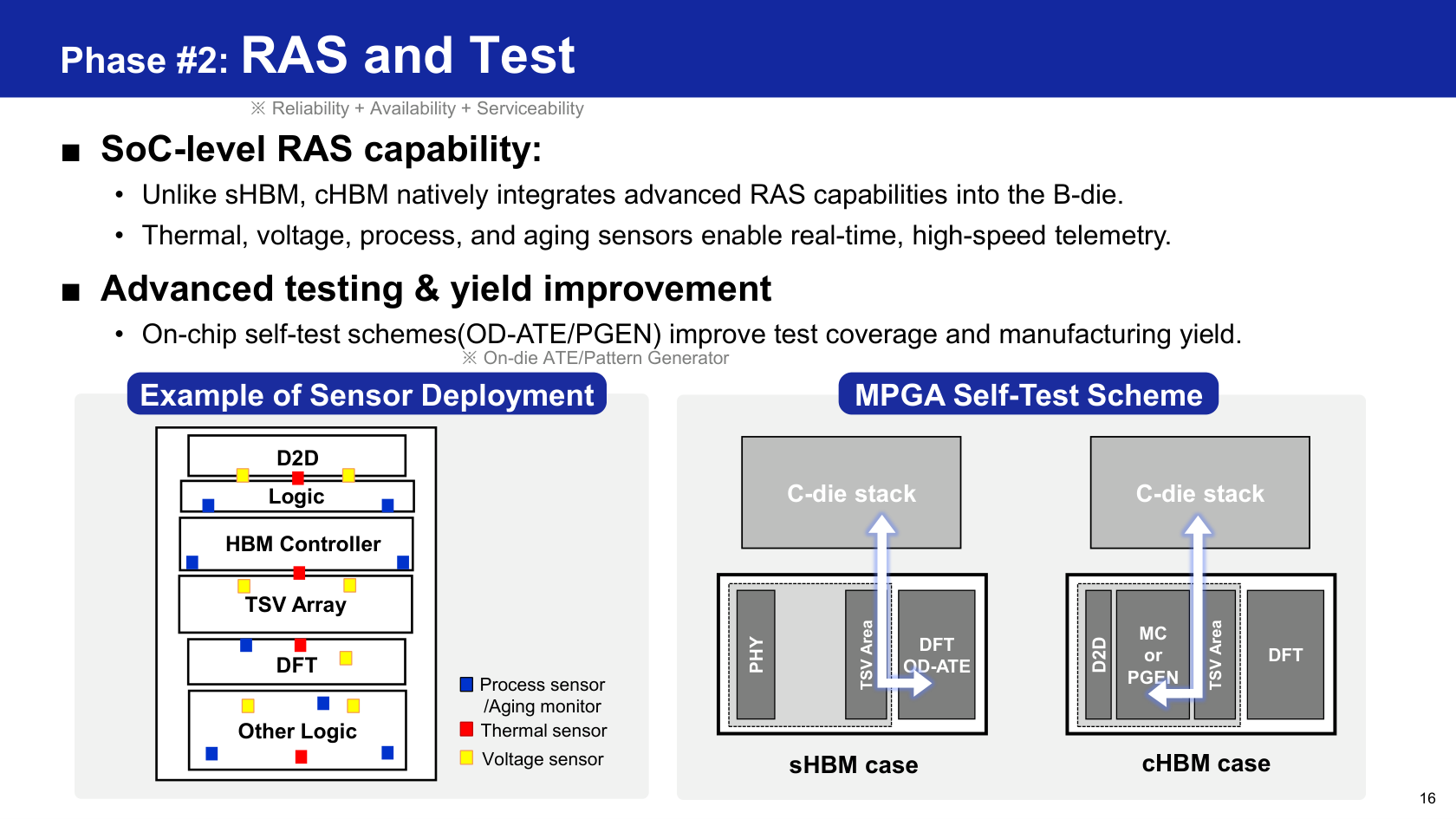
- The colored squares on the left locate sensors around the base-die circuitry: red for temperature, yellow for voltage, and blue for process / aging monitoring. Their readings help identify hot regions or abnormal operating conditions.
- On the right, the arrows trace test patterns from the base-die test circuitry or controller into the core-die stack.
Connect additional memory
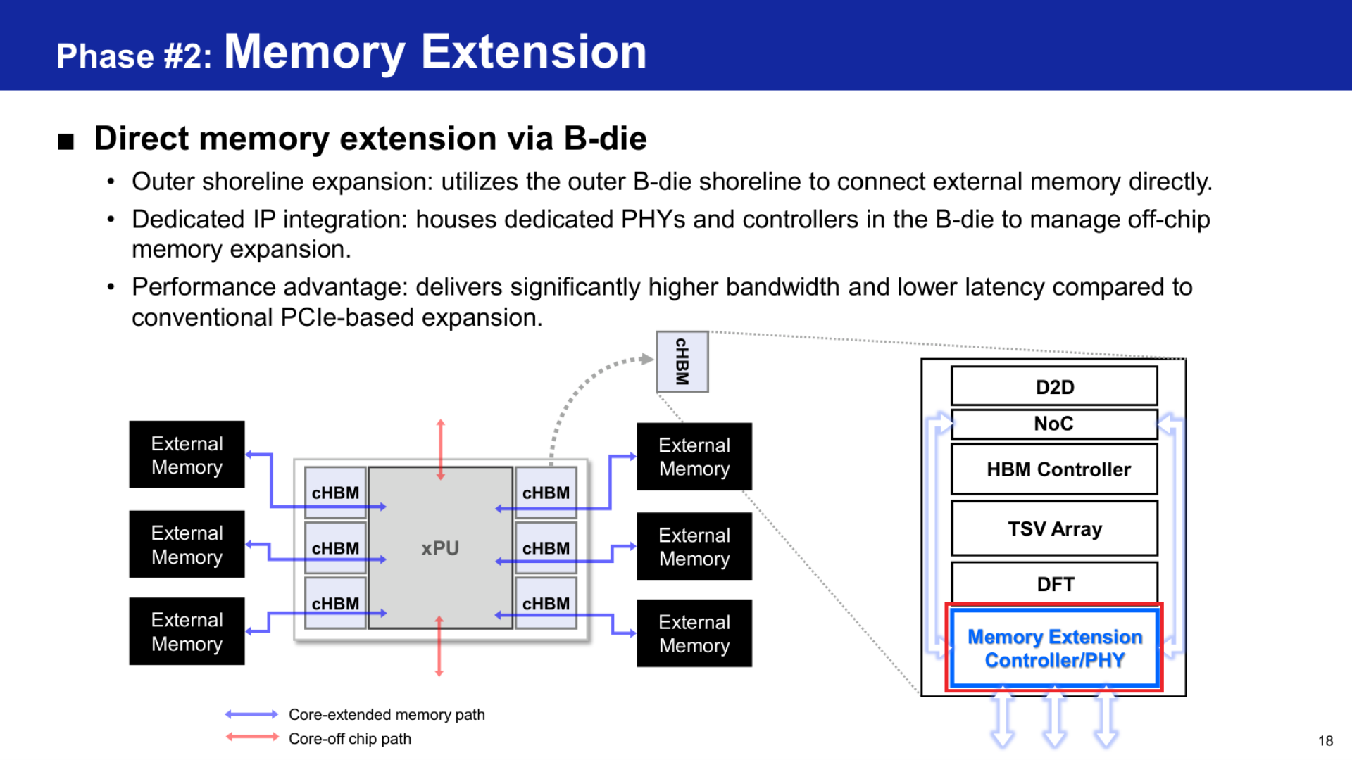
- Space along the base die's outer edge can hold an extension controller and electrical interface for memory outside the HBM stack.
- The left diagram connects the xPU through custom HBM to the black External Memory blocks.
- Follow a request through the right-hand layout:
- Enter the base die through D2D, the die-to-die interface to the processor.
- Cross NoC, the internal network that routes requests and returned data.
- Reach the red-outlined Memory Extension Controller / PHY block. The PHY handles electrical signaling.
- Cross the external link to the additional memory. Returned data follows the connection back.
- This adds storage capacity. Its access delay and bandwidth depend on the attached memory and the connecting path, so the additional memory does not automatically operate at HBM-stack speed.
Compute selected results near the data
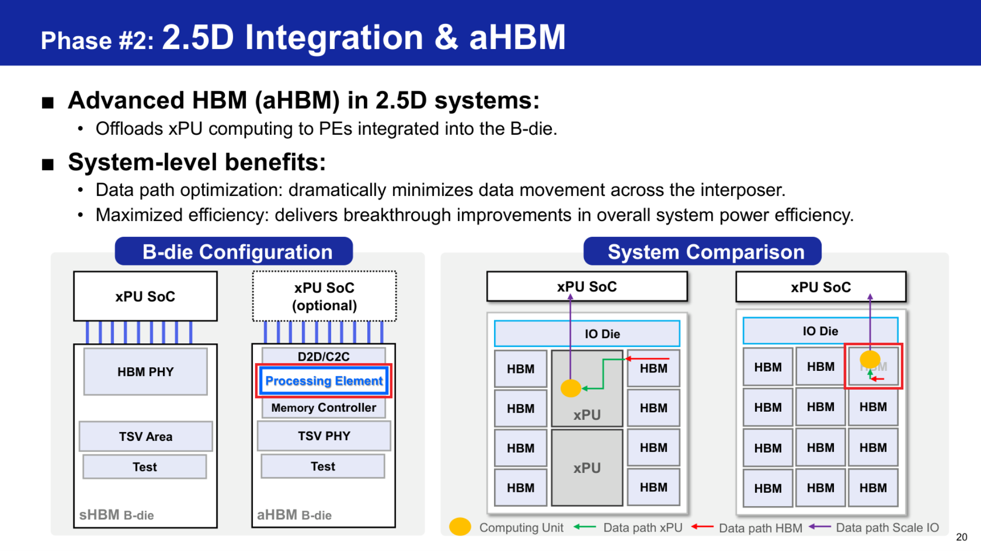
- The red-outlined Processing Element block adds compute beside the memory controller in advanced HBM (aHBM).
- The yellow computing marker moves from the xPU into the red-outlined HBM block on the right, shortening the green path for that work.
- As an illustration, local circuitry could read many stored values, sum them, and return only the smaller result.
- Samsung proposes selected memory-bound attention work for this path. Compute-heavy prefill and feed-forward work remains on the xPU.
- Software must assign suitable operations to those circuits. Reduced data movement must justify their added area, power, and heat beneath the DRAM stack.
3) Phase 3: zHBM places memory vertically above the processor
Change the physical path between memory and compute
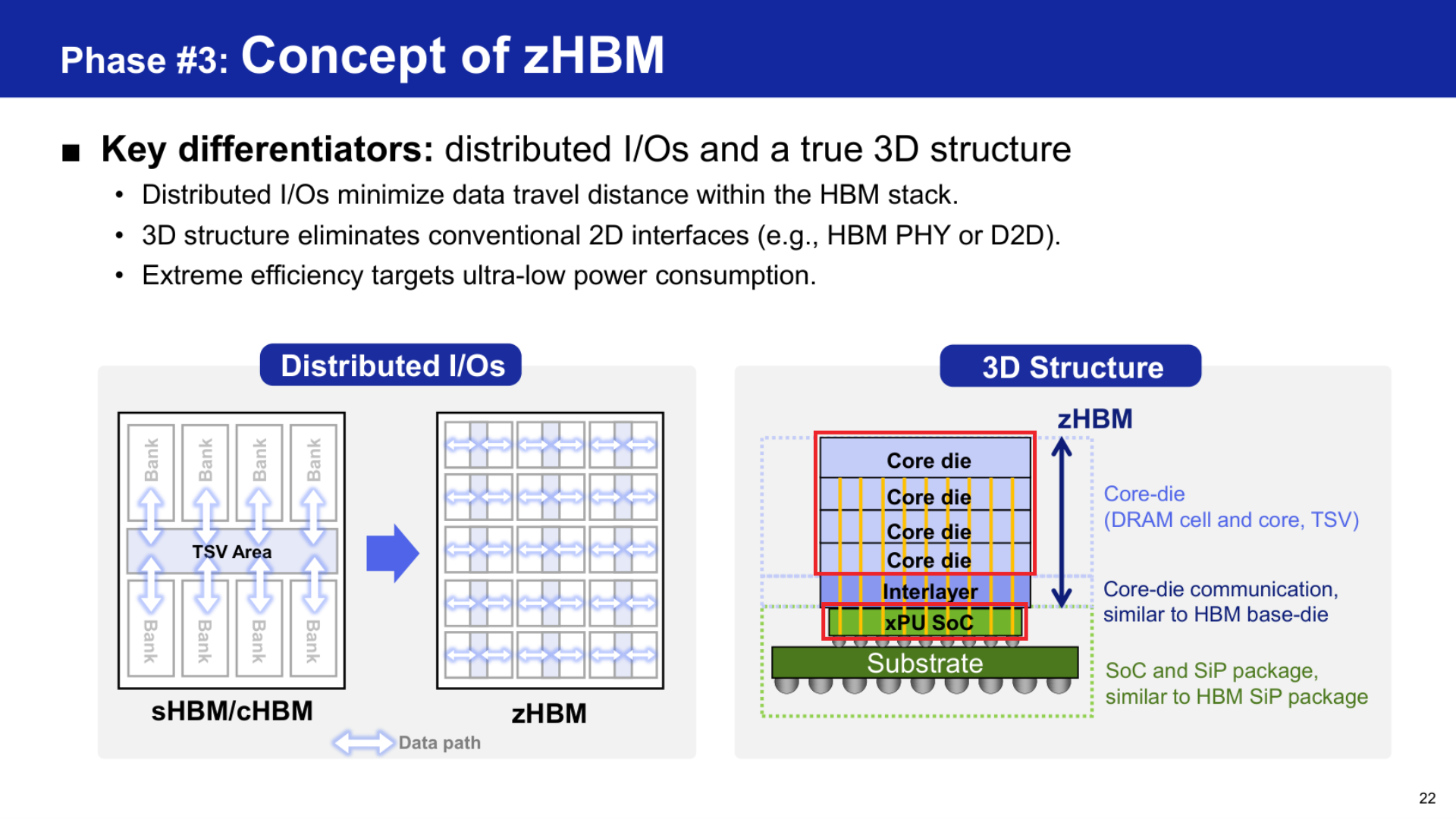
- Standard and custom HBM already stack DRAM dies vertically. However, the memory stack sits beside the processor.
- Data travels sideways between them through the interposer, the wiring layer under the chips.
- zHBM instead places the DRAM core dies above the processor. The red boxes in the right cross-section locate the storage dies above the green xPU.
- In the right cross-section, the interlayer provides communication with the storage dies, similar to an HBM base die.
- The yellow vertical connections carry data toward the green xPU below, aiming to replace the conventional lateral interface.
- The left comparison shows a second change inside the memory die.
- Standard / custom HBM gathers bank traffic toward a central TSV area. TSVs are electrical connections that pass vertically through silicon.
- zHBM distributes these connections across smaller regions. The shorter arrows show data traveling less distance within the memory die before reaching a vertical connection.
- Together, shorter internal routes and a direct vertical processor connection aim to reduce the energy spent moving data. zHBM therefore changes both where memory sits and how data reaches the processor.
Understand the proposed system benefit
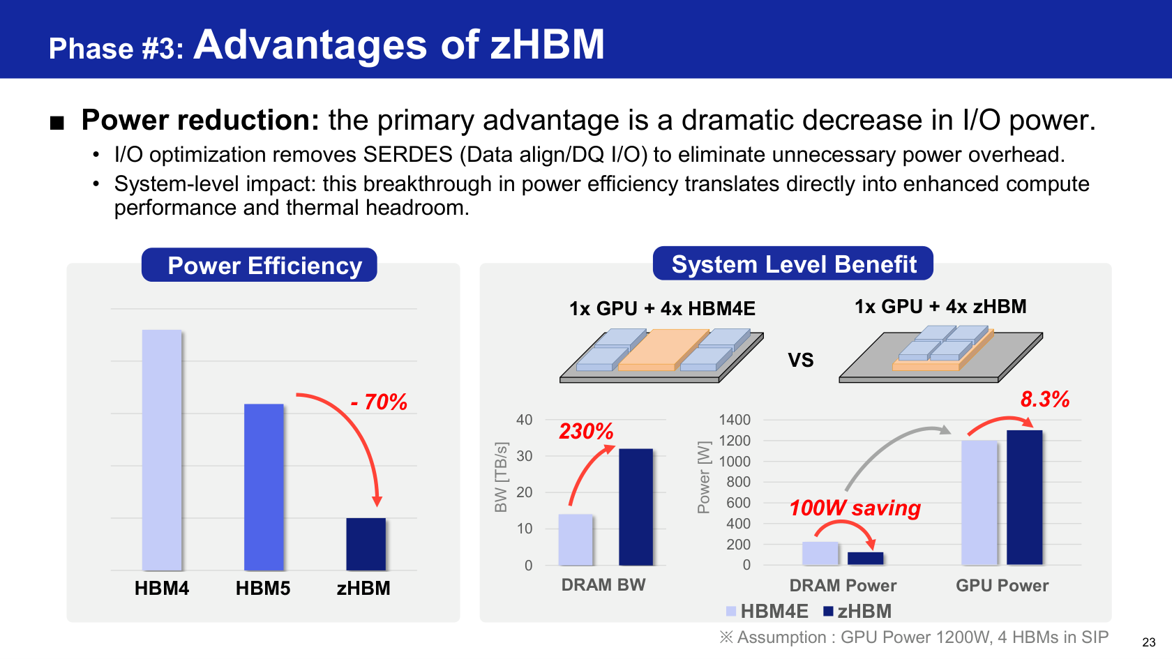
- The left chart compares HBM4, HBM5, and zHBM and marks a proposed 70% power reduction from HBM5 to zHBM. Its vertical axis has no numerical units, so it does not supply an absolute wattage comparison.
- The right charts use a different baseline: one GPU with four HBM4E stacks, shown in pale blue on the chart, versus four zHBM stacks in dark blue.
- The bandwidth axis is in TB/s. The bars illustrate roughly 2.3 times the baseline bandwidth
- The power axis is in watts. The example reallocates a modeled 100 W memory-power saving to a GPU initially budgeted at 1,200 W, increasing its budget to 1,300 W.
- Lower memory power leaves more of the package budget available for GPU computation. The performance benefit depends on whether the workload can use that additional power.
- These are architectural targets and modeled comparisons, rather than measurements of a shipping zHBM system. Making the vertical arrangement practical also requires dense bonding, cooling, and joint memory–processor design and verification.
(2) SK hynix: build taller stacks, remove heat, and qualify the complete package
- SK hynix (KRX: 000660) treats HBM scaling as an assembly problem: adding storage layers and electrical connections is useful only if the stack can be manufactured, cooled, and integrated reliably.
- Its approach proceeds from improving the existing solder-based stacking process to hybrid bonding for denser stacks, then addresses hot spots and stresses in the accelerator package.
1) Extend the existing stacking process
Understand the two solder-based assembly methods
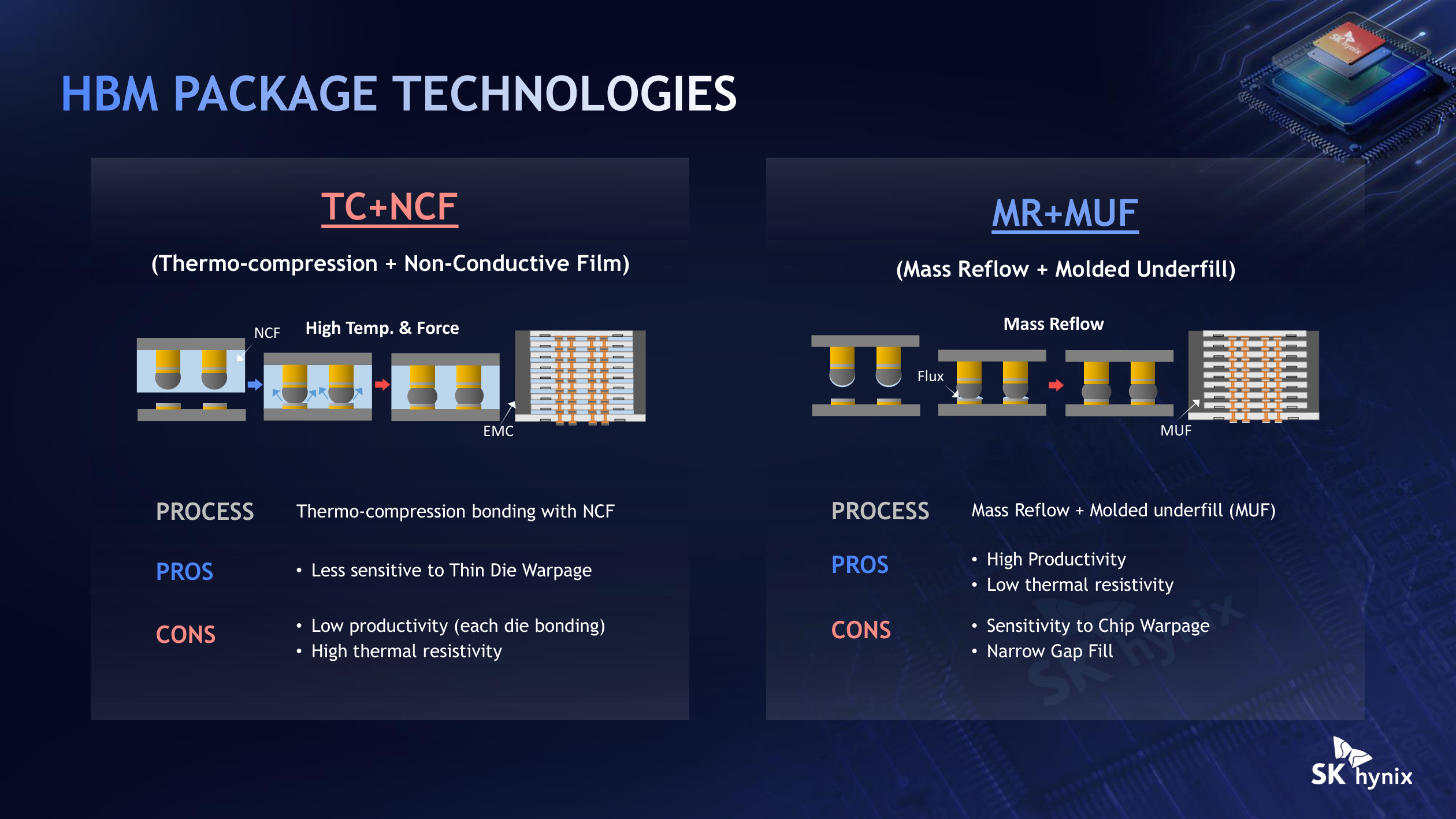
- On the left, TC-NCF bonds the layers individually:
- Place a die with non-conductive film around its electrical joints.
- Apply heat and pressure to bond it.
- Repeat for the next die.
- Supporting each bond reduces sensitivity to thin-die bending, but the repeated steps limit throughput.
- On the right, MR-MUF processes the assembled stack:
- Stack the dies.
- Melt the solder joints during mass reflow.
- Fill the remaining gaps with molded underfill.
- This improves throughput and provides a favorable heat path, but bent dies or unfilled gaps can leave unreliable connections.
- SK hynix's near-term approach improves MR-MUF for narrower gaps, thinner dies and higher layer counts.
Fit 16 layers into nearly the same height
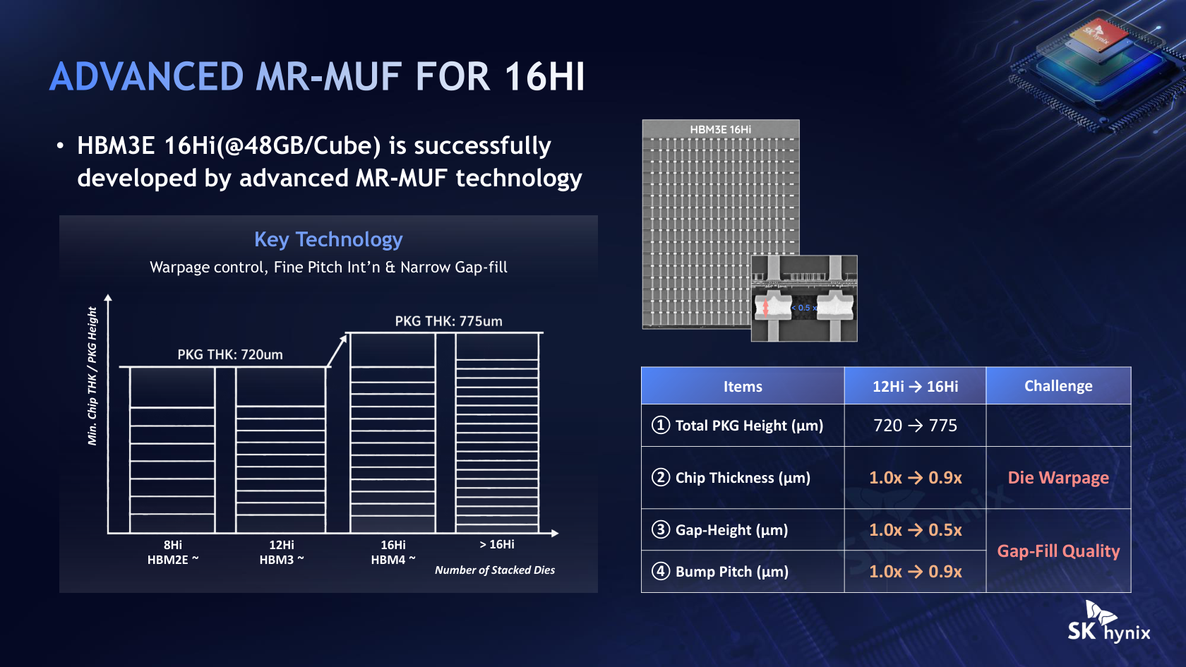
- The table fits four additional storage layers into a package only slightly taller: 16 layers at 775 μm versus 12 at 720 μm.
- The extra layers fit because the illustrated die thickness falls to 0.9 times its reference and the inter-die gap falls to 0.5 times its reference.
- Thinner dies bend more easily, so the joints may not all meet their partners uniformly.
- Narrower gaps are harder to fill completely. An unfilled region can weaken mechanical support or interrupt the intended heat path.
- Controlling die bending, alignment, and gap filling therefore determines how many complete working stacks the process produces.
2) Use hybrid bonding when solder gaps constrain further stacking
Replace the solder gap with directly bonded surfaces
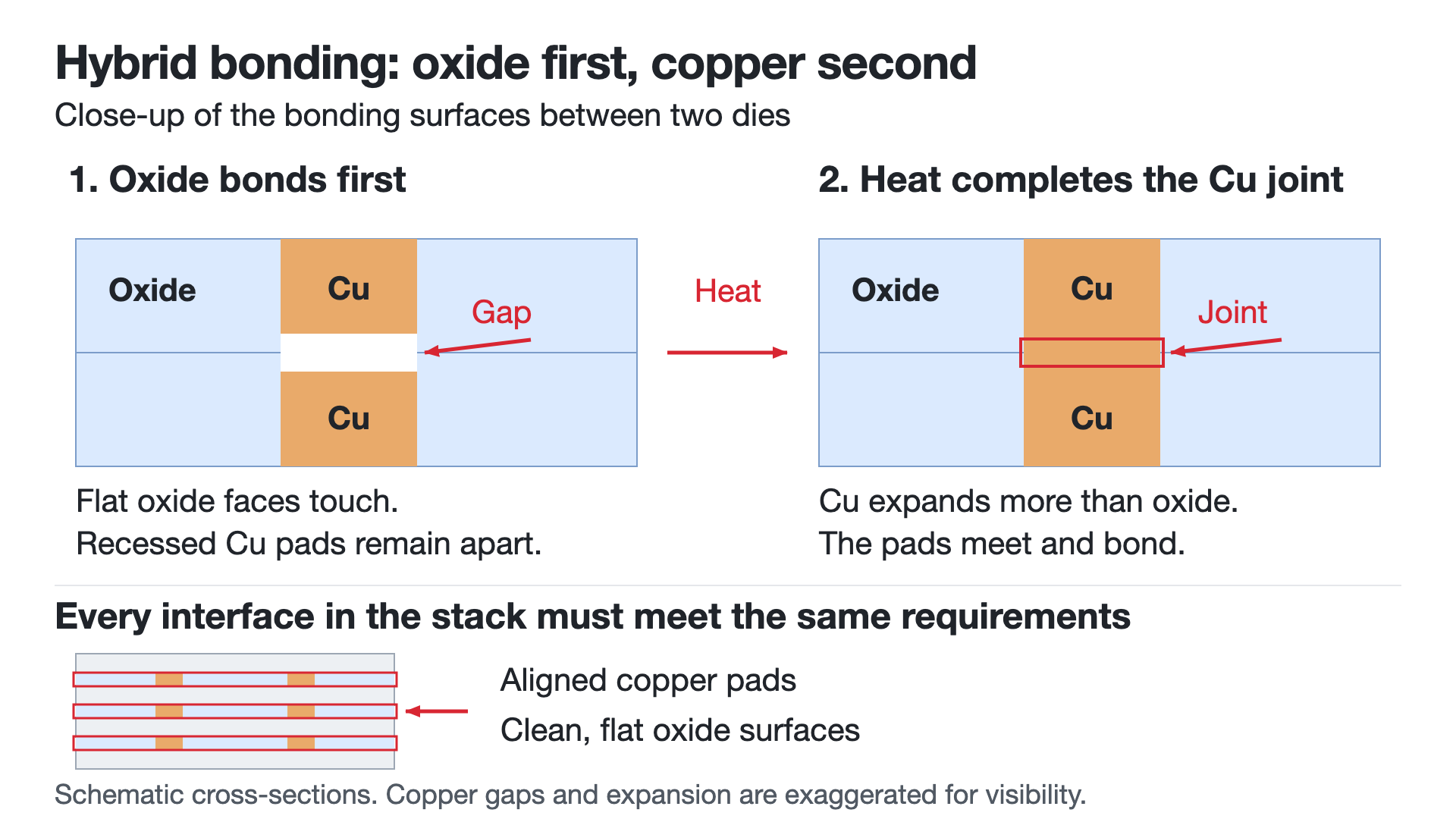
- Hybrid bonding proceeds in two stages:
- First, flat oxide surfaces contact. The copper pads remain slightly recessed.
- During heating, copper expands more than the oxide and completes the electrical joints.
- Removing the protruding solder gap leaves more height for storage dies or additional layers.
- Directly joined surfaces and metal connections also change the path through which heat crosses each interface.
- Every interface must meet the alignment and surface-quality requirements. One particle or misaligned pad can interrupt a required connection in the completed stack.
Read the capacity and cooling roadmap together
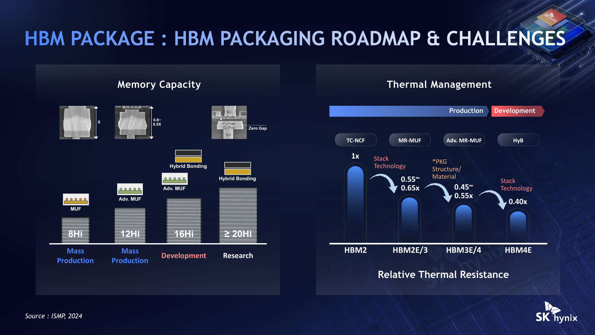
- The left progression moves from molded-underfill stacks toward hybrid bonding for 20 or more layers. This is a process roadmap, with production and development categories inherited from the slide's ISMP 2024 reference.
- The right blue bars describe relative thermal resistance: how much temperature rise occurs above the cooling surface for a given heat load.
- TC-NCF is the 1.0 reference, and the hybrid-bonding target is 0.40. At the same heat load, that corresponds to 60% less temperature rise along the compared thermal path.
3) Give growing power and local hot spots a heat-removal path
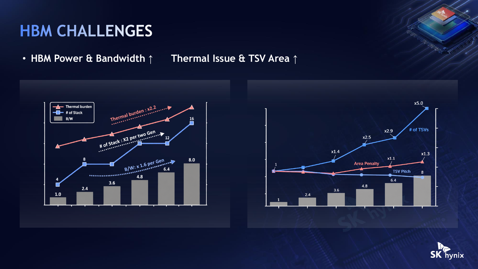
- In the left trend diagram, the gray bandwidth bars and blue layer-count line rise together, while the red thermal-burden line also rises. More storage and faster transfers create additional heat that must leave the stack.
- On the right, more TSV connections occupy die area even as their spacing narrows. TSVs are vertical electrical connections through silicon, so adding them requires both routing space and manufacturing steps.
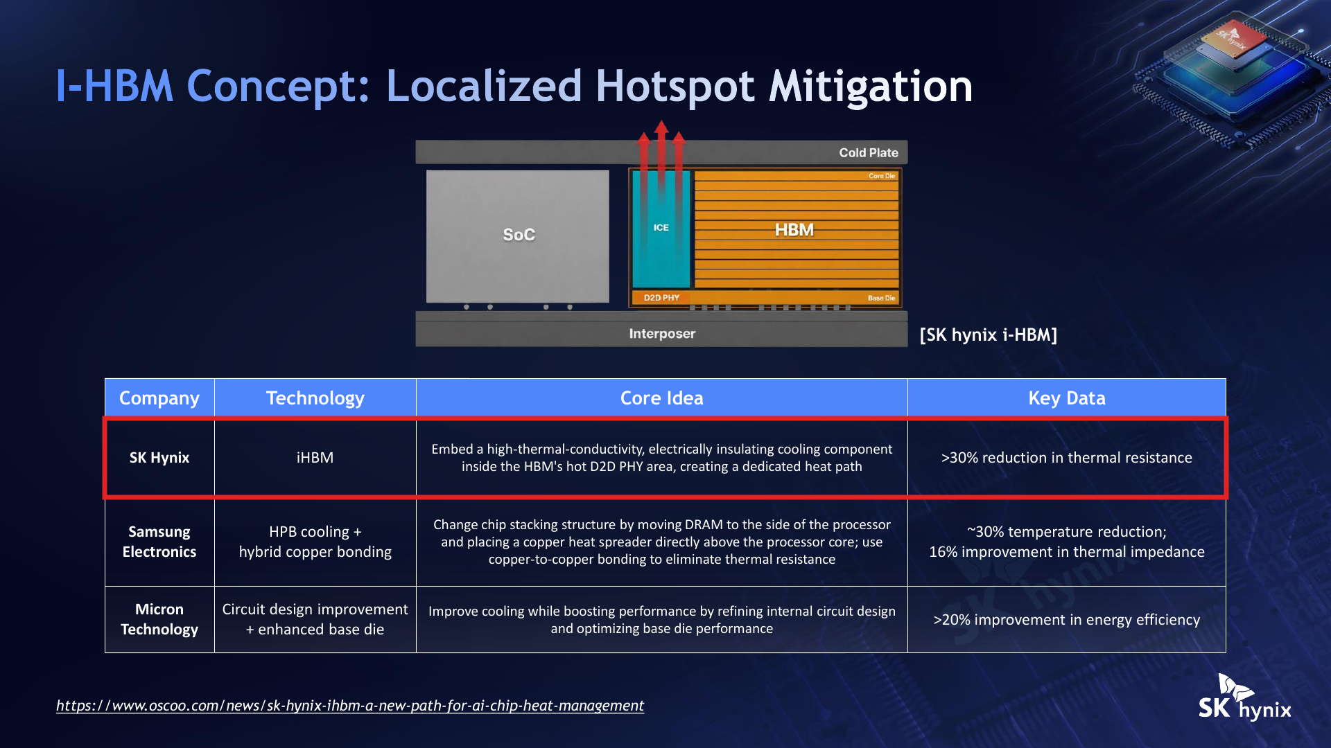
- The orange D2D PHY region drives the signals between chips and creates a concentrated hot spot. The teal cooling element, ICE, sits directly above it beside the storage layers.
- The red arrows trace heat from this element toward the cold plate. That dedicated route reduces how much interface heat must pass through the temperature-sensitive DRAM stack.
- The red rectangle marks the SK hynix row, which reports more than 30% lower thermal resistance for the i-HBM concept.
4) Qualify HBM inside the accelerator's assembly flow
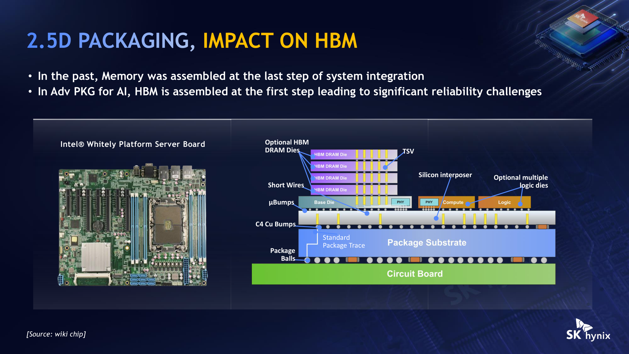
- The left example mounts memory on a server board. The right places HBM beside compute dies on an interposer inside one package.
- HBM is attached early in the package's assembly flow.
- Later heating, bonding and mechanical stresses can damage a stack that passed its own earlier tests.
- The memory supplier and package assembler must therefore qualify the complete combination through assembly and operation, including the interposer and surrounding materials.
- SK hynix names TSMC (NYSE: TSM) as its logic-foundry partner for HBM4 base dies. The two companies also collaborate on integrating SK hynix HBM with TSMC’s CoWoS accelerator packaging.
- SK hynix reported HBM4 mass shipments beginning in Q2 2026. Logic-foundry capacity and complete-package qualification now sit alongside DRAM stacking in the route to deliverable HBM.
(3) d-Matrix: make vertical DRAM bandwidth usable for low-latency inference
- d-Matrix's Raptor targets decode workloads that repeatedly read weights and attention state while producing each user's next token. At the small batches used for fast responses, data delivery can leave arithmetic waiting.
- Raptor puts logic directly above DRAM to prioritize rapid delivery over storage density. That choice makes cooling and fast communication between capacity-limited devices part of the design.
1) Choose the memory layout and connect the compute devices
Trade some capacity density for a broad vertical data path
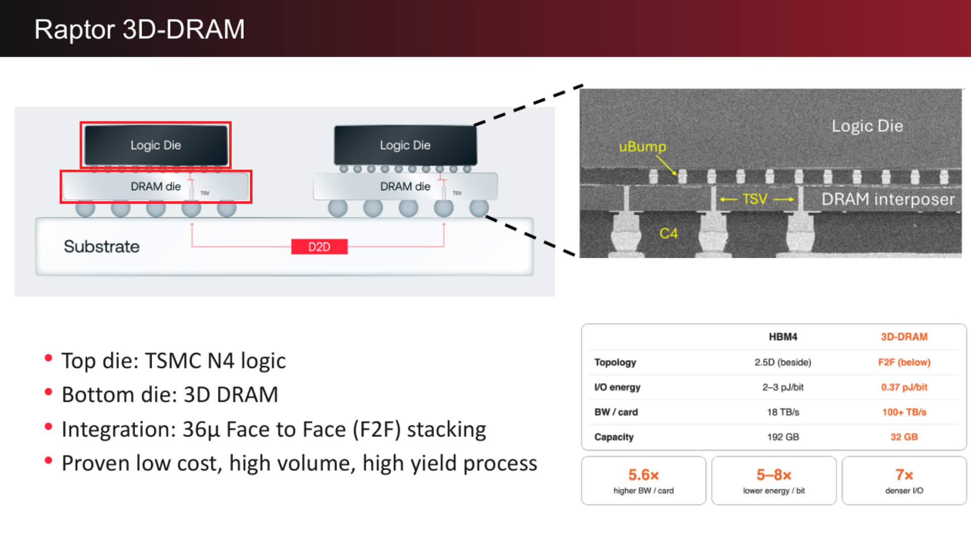
- The two red boxes on the left locate Raptor’s logic die above its DRAM die, joined across their facing surfaces by microbumps. Data reaches compute through many short vertical connections rather than traveling sideways to an HBM stack.
- The logic uses TSMC’s 4 nm-class process.
- The table compares more than 100 TB/s at 32 GB per Raptor card with 18 TB/s at 192 GB in the HBM4 example: roughly 5.6 times the bandwidth, with one-sixth the capacity.
- Logic on top gives its heat a shorter route to the cooler. Power and external signals must instead pass through the DRAM's vertical connections. The disclosed cooling case uses a one-high structure with liquid cooling.
Keep communication from replacing memory as the main wait
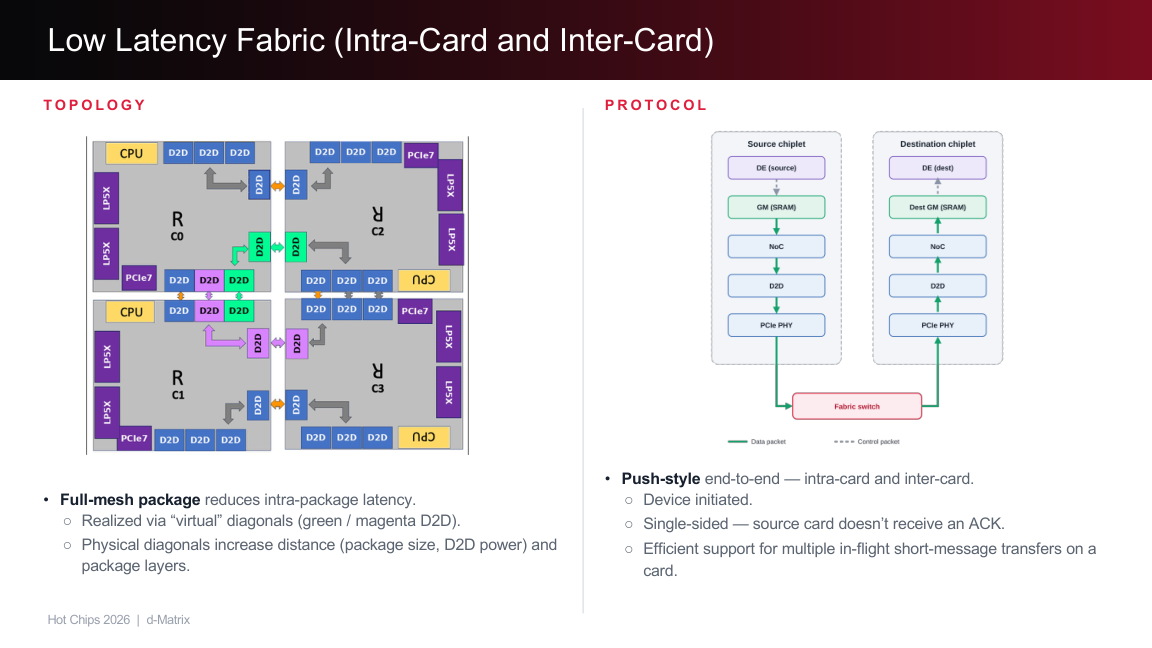
- The left topology connects four chiplets through local die-to-die links, including the green and purple virtual diagonals. These provide the desired connectivity without drawing long physical diagonal wires across the package.
- The right-hand flow starts in the sender's SRAM.
- Data crosses the internal network and external fabric, then arrives in destination SRAM.
- The sender can start several short messages before earlier ones finish, allowing transfers to overlap other ready work.
- A large model still spans multiple devices because each card has limited storage.
- A layer waiting for another card's partial result cannot finish merely because its own memory is fast. The short-message fabric therefore contributes to the low-latency design.
2) Evaluate the resulting bandwidth and capacity together
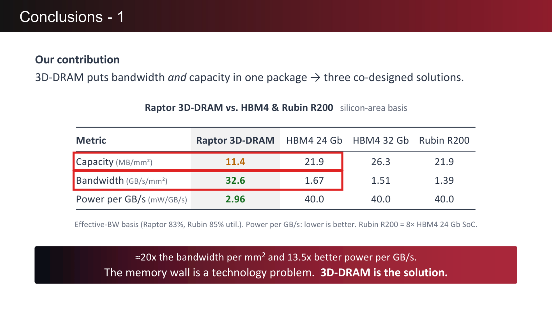
- The red rectangles compare capacity and bandwidth per unit of silicon area. Against the HBM4 24-Gb column, Raptor lists 11.4 versus 21.9 MB/mm² of capacity, but 32.6 versus 1.67 GB/s/mm² of bandwidth.
- That is approximately 19.5 times the bandwidth per area with less storage per area. The power row is mW per GB/s, so a lower value means less power for the same delivered data rate.
- The table assumes 83% effective-bandwidth utilization for Raptor and 85% for Rubin.
Limit the power and refresh cost of the wide memory link
- Raptor can store a bit pattern in inverted form when that reduces switching on the link, then restore it when read. A tag stored with the error-correction metadata records the choice. d-Matrix reports about 20% lower I/O power, rather than a 20% reduction in total chip power.
- Hotter DRAM needs more frequent refresh to retain data. Raptor divides memory into many banks with fewer rows per bank, shortening each refresh operation. Its disclosed 105°C case uses refresh eight times as frequently while losing less than 1.4% of bandwidth.
4. OXMIQ: cheap capacity can still make expensive tokens
- High-Bandwidth Flash (HBF) places NAND flash near compute with a much wider connection than a conventional SSD, aiming to provide a larger, cheaper memory tier.
- OXMIQ Labs and PRAXMATI examine three deployment choices: HBM alone, HBF alone, and a mixed system that keeps active data in HBM.
- Cheaper memory can still produce more expensive tokens if the GPU spends more time waiting for data. The system continues to incur hardware and operating costs while producing fewer tokens.
- The analysis uses proposed hardware specifications and simulations. Its results describe the modeled configurations, rather than a deployed HBF inference fleet.
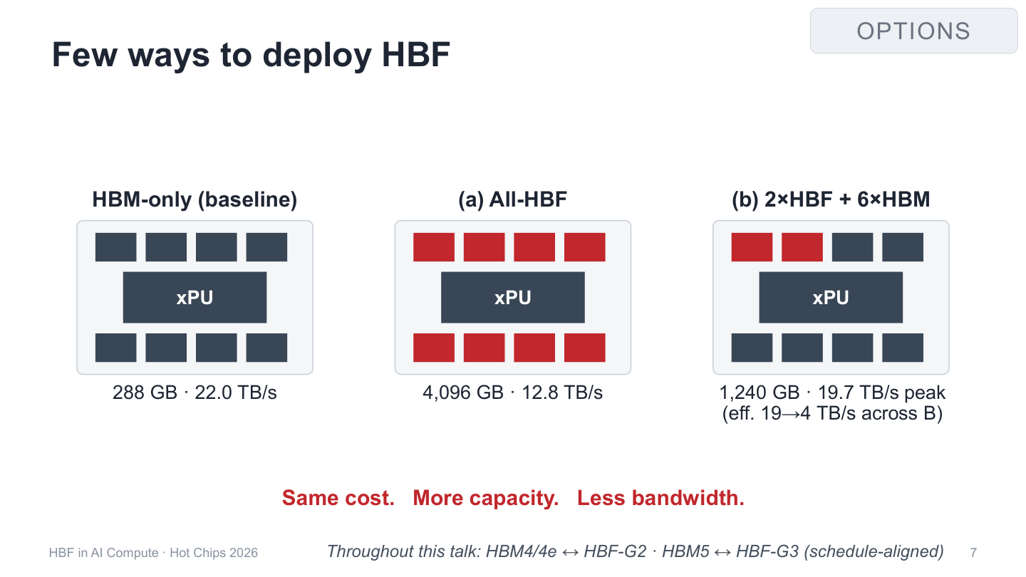
- The gray HBM-only configuration provides 288 GB and 22.0 TB/s per xPU.
- Replacing it with the red HBF blocks raises modeled capacity to 4,096 GB but lowers bandwidth to 12.8 TB/s.
- The mixed configuration combines six HBM stacks with two HBF cubes. Frequently used data stays in HBM; HBF holds the larger backing pool.
- Its 19.7 TB/s peak adds the tiers' maximum rates. A needed expert stored only in HBF still depends on HBF's path.
- Unused HBM bandwidth cannot fetch that expert faster. Effective delivery on the slide falls toward 4 TB/s as the batch's access pattern changes.
(1) Match stored capacity to the active data
- A larger capacity tier can help when the workload stores much more data than it reads during each inference step. MoE weights and a long attention history can have this property, but their read demand depends on how requests are served.
Mixture of experts: store many networks, activate selected ones
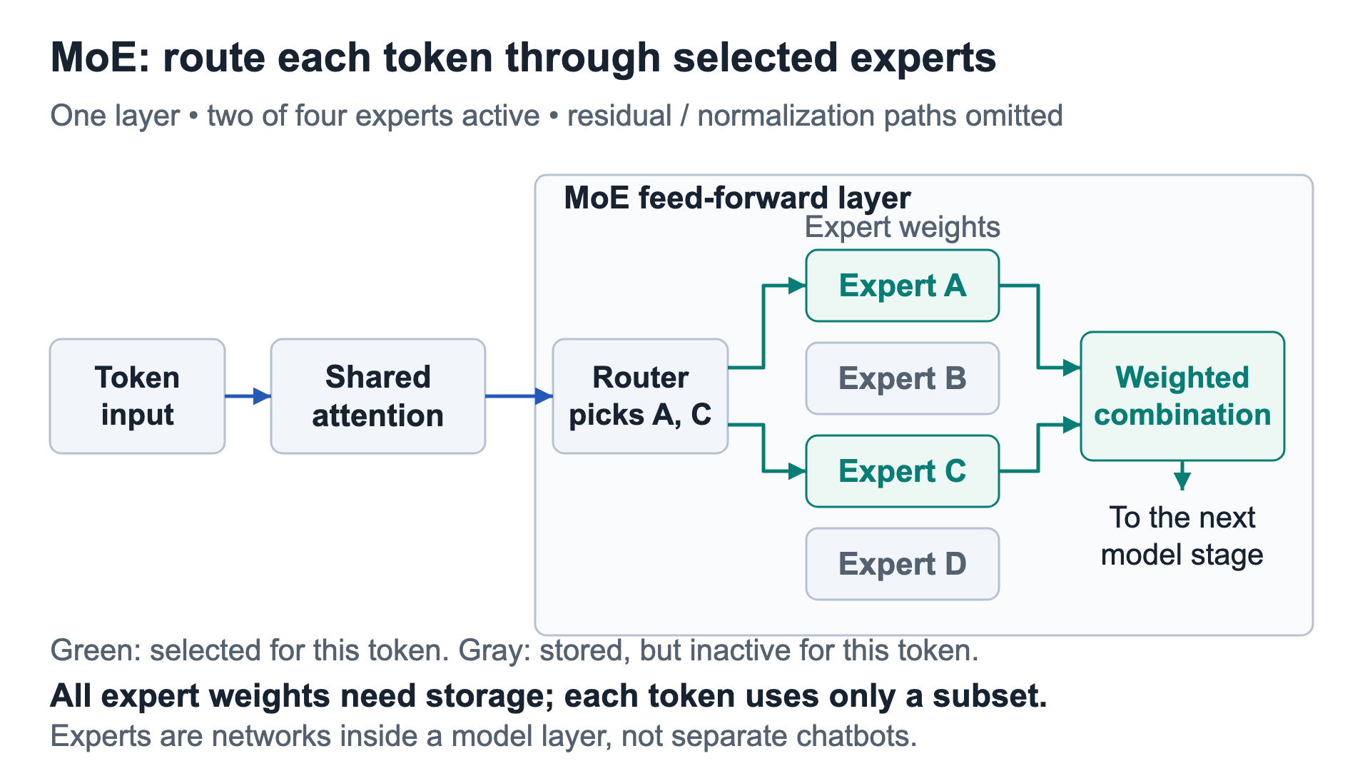
- A mixture-of-experts (MoE) model stores many expert networks, but activates only a subset for each token.
- Follow the diagram in order:
- The token representation passes through shared attention.
- The router selects experts A and C, shown in green.
- Those feed-forward networks process the input; B and D remain inactive.
- Their outputs are combined before the representation continues to the next stage.
- The diagram omits normalization and residual paths. Stored expert capacity can be much larger than the weights used for one token.
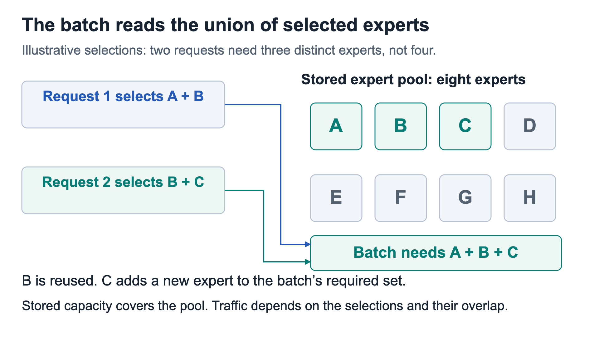
- The memory system must hold all expert weights, but each token uses only the selected experts at that layer. This creates a possible role for a larger capacity tier, provided selected weights reach compute quickly enough.
- In the batch example, request 1 needs A + B and request 2 needs B + C. Serving them together requires A + B + C: B can be reused, but C adds another expert to read.
- As more requests join a batch, the group can select more distinct experts. A small active fraction for one token does not guarantee little memory traffic for the whole batch.
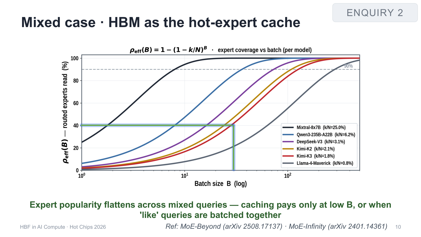
- The horizontal axis is batch size on a logarithmic scale. The vertical axis is the percentage of experts read at least once across the batch.
- The black Mixtral curve approaches full expert coverage at a smaller batch than the gray Llama-4-Maverick curve, because each Mixtral token selects a larger share of its expert pool in this comparison.
- For a mixed HBM / HBF system, broader expert coverage means that more requested weights may fall outside the subset kept in HBM. More of the batch then depends on the slower HBF path.
- The curves assume uniform, independent expert selection. Frequently reused experts or requests with similar selections can improve reuse, although waiting to group requests can delay responses.
- Batch throughput versus user speed: Reusing weights across more requests can increase total tokens produced per second, while the longer batch step can make each user wait longer for their next token.
Sparse attention: keep a long history, read selected context
- Sparse attention can retain a long KV history while reading selected entries. The KV cache stores keys and values from earlier tokens so attention can reuse that state during generation.
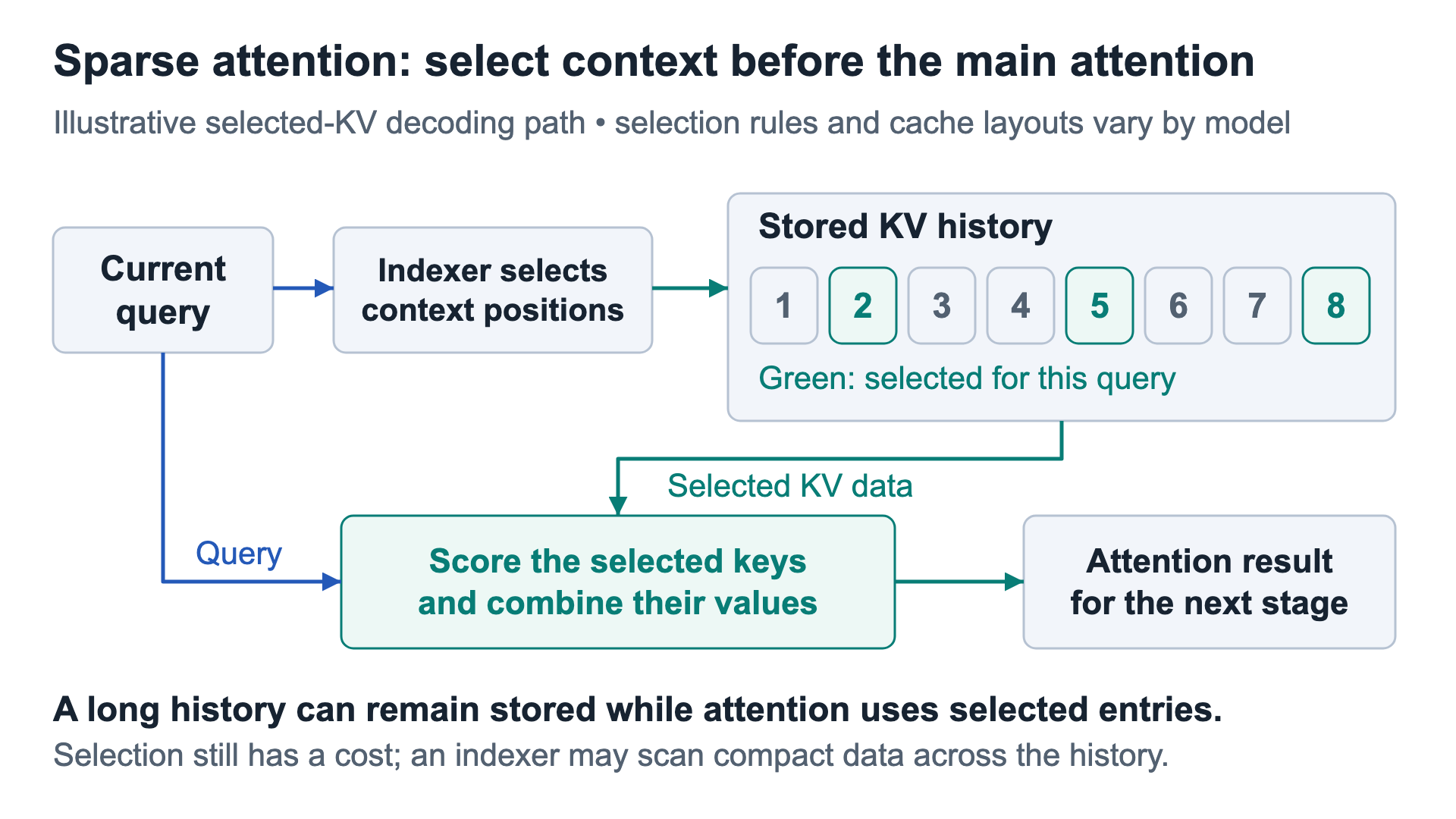
- The blue query represents the current token's information request.
- The illustrated indexer selects positions from the stored KV history.
- The green path brings those entries into attention.
- Attention scores their keys, then combines their values into the result.
- Stored context can be much larger than the context used by one attention operation. Unselected entries stay in the cache for later queries.
- Selection overhead: Finding the relevant entries still takes computation and memory reads.
- Read amplification: Scattered entries can require reading extra flash data, so placement and buffering matter.
(2) Both capacity and bandwidth matter
Having enough memory to hold a model does not guarantee that the memory can feed data to the GPU fast enough.
- Capacity: Can the memory hold all the model weights and KV cache?
- Bandwidth: Can it deliver that data quickly enough to meet the response-time target?
- Suppose a workload needs 500 GB of storage. The following configurations are illustrative.

- The second unit might be purchased for its additional data-transfer path, even though the workload does not need its extra storage space. This assumes the system can spread the reads across both units.
- A low price per GB does not automatically mean a cheaper deployment: a cheaper but slower memory option may require more units to achieve the required performance.
- HBF must supply the bytes each step needs quickly enough to meet the response target, as well as hold the model.
- Otherwise, buying additional hardware for speed can reduce the expected savings.
What can turn a capacity problem into a bandwidth problem?
- Faster responses: The same model data must arrive in less time for each decode step, raising the required bandwidth.
- More concurrent requests: A batch can need more distinct expert weights and more users' KV data, although shared weights can be reused.
- Longer context: Retaining more KV history increases storage demand. Its read demand depends on whether attention uses the full history or selects a smaller portion.
- In the short-context simulation, one HBF-equipped GPU can hold the model even with much of its storage unused. As the requested token rate or read volume rises beyond that GPU's bandwidth, additional hardware is needed.
- Longer context requires more KV storage. Whether HBF lowers system cost also depends on its read rate and the required response time.
(3) Separate instance size from rack economics
1) Fewer GPUs per instance can leave room for more copies
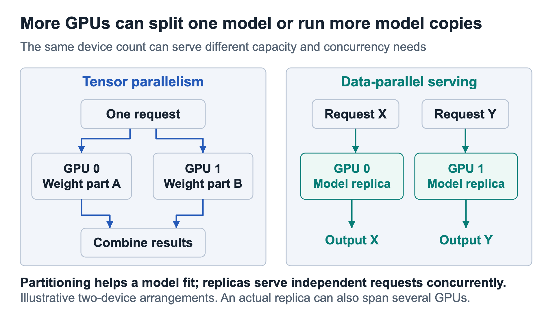
- Left: two GPUs run one model instance. Each GPU holds a different portion of the model weights. They perform their parts of the calculation and combine the results to serve the same request.
- If one GPU can run that instance: The second GPU becomes available to run another complete copy of the model.
- Right: two model copies serve separate requests. Each GPU runs its own instance, allowing the system to serve different requests independently.
- One GPU must still run the model fast enough, not merely have enough memory to hold it. Using fewer GPUs reduces the combined compute and memory bandwidth available to each instance, so it must still meet the response-time target.
2) Compare the same rack, not just the number of copies
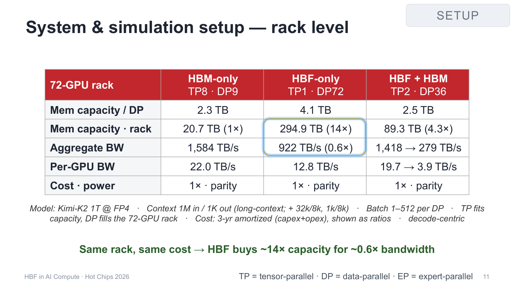
- The simulation holds the rack at 72 GPUs and assumes equal rack cost and power.
- The modeled workload is Kimi-K2 at FP4, with long contexts and varying batches.
- TP, or tensor parallelism, identifies how many cooperating GPUs split one instance's calculations.
- DP, or data parallelism, identifies how many independent model copies run in the rack.
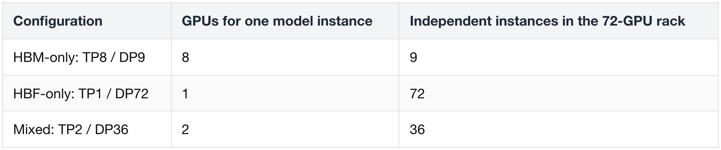
- More copies do not guarantee more tokens per second: each copy still depends on its available compute and memory bandwidth.
- The highlighted HBF-only rows show about 14 times the rack's storage but only about 0.6 times its aggregate memory bandwidth, relative to HBM-only.
- “Mem capacity / DP” is memory per model instance. The rack total adds the memory of all those separate copies; replicated weights occupy space in each copy.
- “Aggregate BW” adds the GPUs' local memory bandwidth. It does not measure the network bandwidth between GPUs.
3) A lower entry cost can coexist with a higher token cost
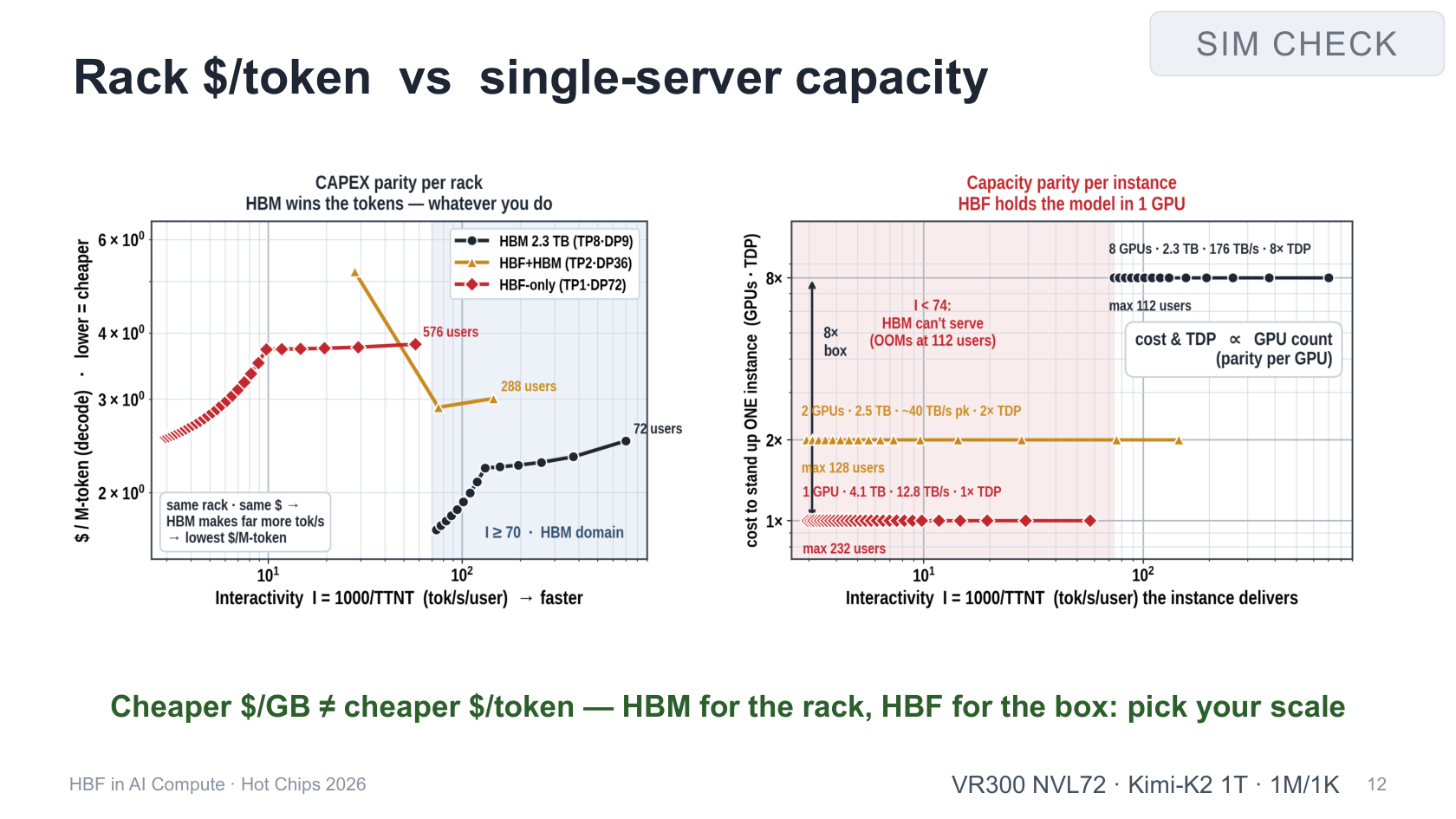
Read both plots from left to right: Their horizontal axis is tokens per second per user, on a logarithmic scale. Farther right means each user receives a faster response.
Left: cost of output from a full rack. The vertical axis is dollars per million decode tokens, so lower is cheaper.
- Black circles represent HBM, red diamonds HBF, and gold triangles the mixed system (HBM + HBF).
- Where the curves cover the same response speed, HBM's black curve is lower in this simulation. The modeled rack produces more tokens at that speed, spreading its cost across more output.
Right: hardware needed to run one model instance. The vertical axis is GPU count and proportional cost / power under the model's assumptions.
- HBF fits the instance on one GPU, the mixed system uses two, and HBM uses eight.
- HBF's red line is lower on the right because it needs less hardware for one instance. Its line also ends at a slower response speed than HBM's: the extra storage does not replace the bandwidth supplied by the eight-GPU HBM instance.
- The curves vary the number of users. HBM's missing slow-response region reflects an out-of-memory limit at high concurrency in the simulated setup, rather than an inability to serve fewer users slowly.
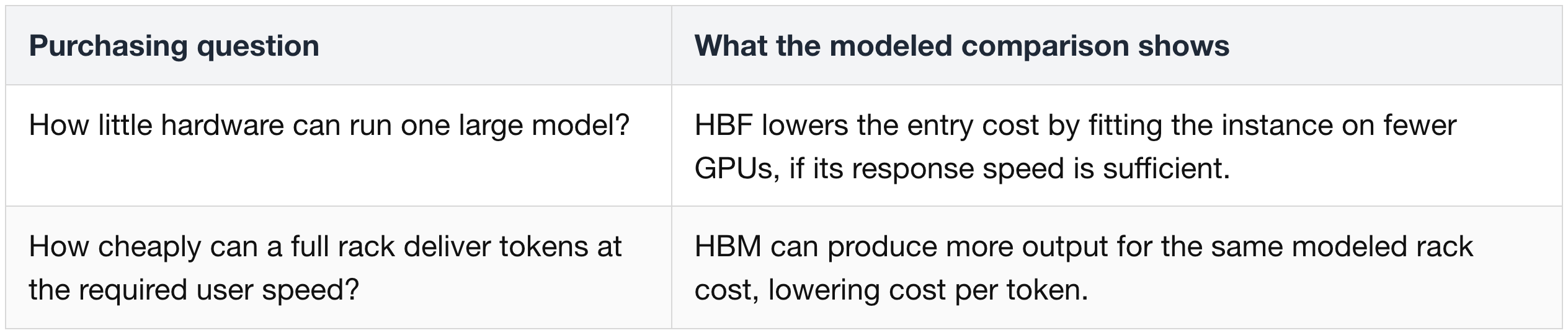
- Fitting a model cheaply and serving its tokens cheaply are different outcomes. HBF's capacity advantage is strongest when the workload benefits from stored data that does not all need to be read continuously.
(4) Stage data before computation needs it
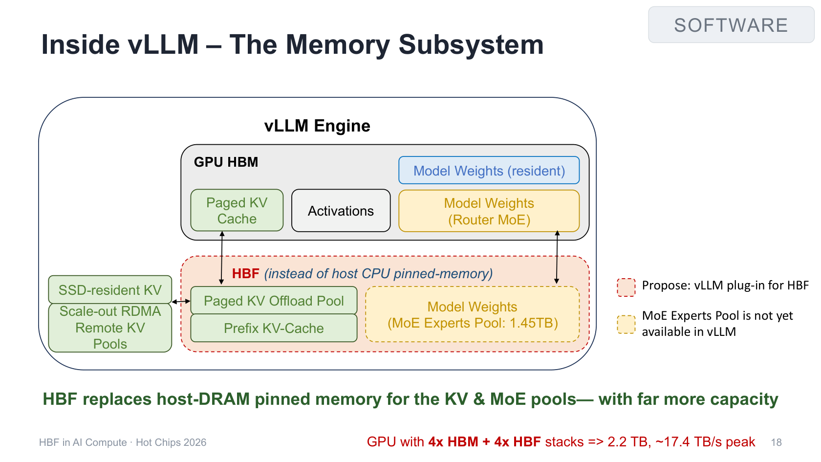
- Upper gray region: the active working data. GPU compute uses the KV entries, activations and resident weights held in HBM.
- Lower HBF region: the larger backing pool. It holds offloaded KV history, reusable prefix KV and a proposed expert-weight pool. The arrows bring selected data into HBM before computation needs it.
- The dashed HBF boundary identifies a proposed vLLM plug-in. The dashed expert pool is marked as not yet available in the depicted software.
- This four-HBM / four-HBF software example differs from the six-HBM / two-HBF configuration used in the earlier mixed-system comparison.
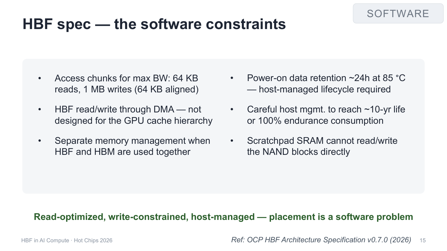
- Transfers: The left column specifies 64 KB reads and 1 MB writes aligned to 64 KB for maximum bandwidth.
- Software can group smaller requests into larger transfers.
- Supporting a small request does not mean that request achieves the peak rate.
- Placement and prefetching: Keep urgent or frequently reused data in HBM.
- Start moving expected data from HBF while other work runs.
- If it arrives late, the GPU still waits.
- Retention: The proposed approximately 24 hours at 85°C is a power-on data-retention specification. The host must manage that lifetime; the figure does not establish how long data remains valid with power removed.
- Write endurance: Repeated rewriting wears the flash. The roughly ten-year target depends on host management, and the write-endurance specification remains unresolved in the presentation.
- HBF lowers inference cost only when its capacity savings outweigh the cost of supplying data fast enough. The outcome depends on bandwidth needs and how software places, transfers and reuses data.
5. What the memory tutorials imply for the industry
- The memory approaches reduce waiting in different ways, each with a different scarce resource.
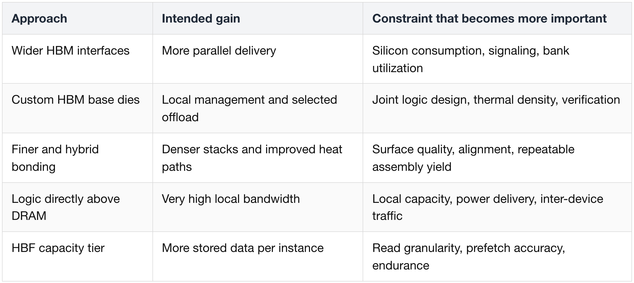
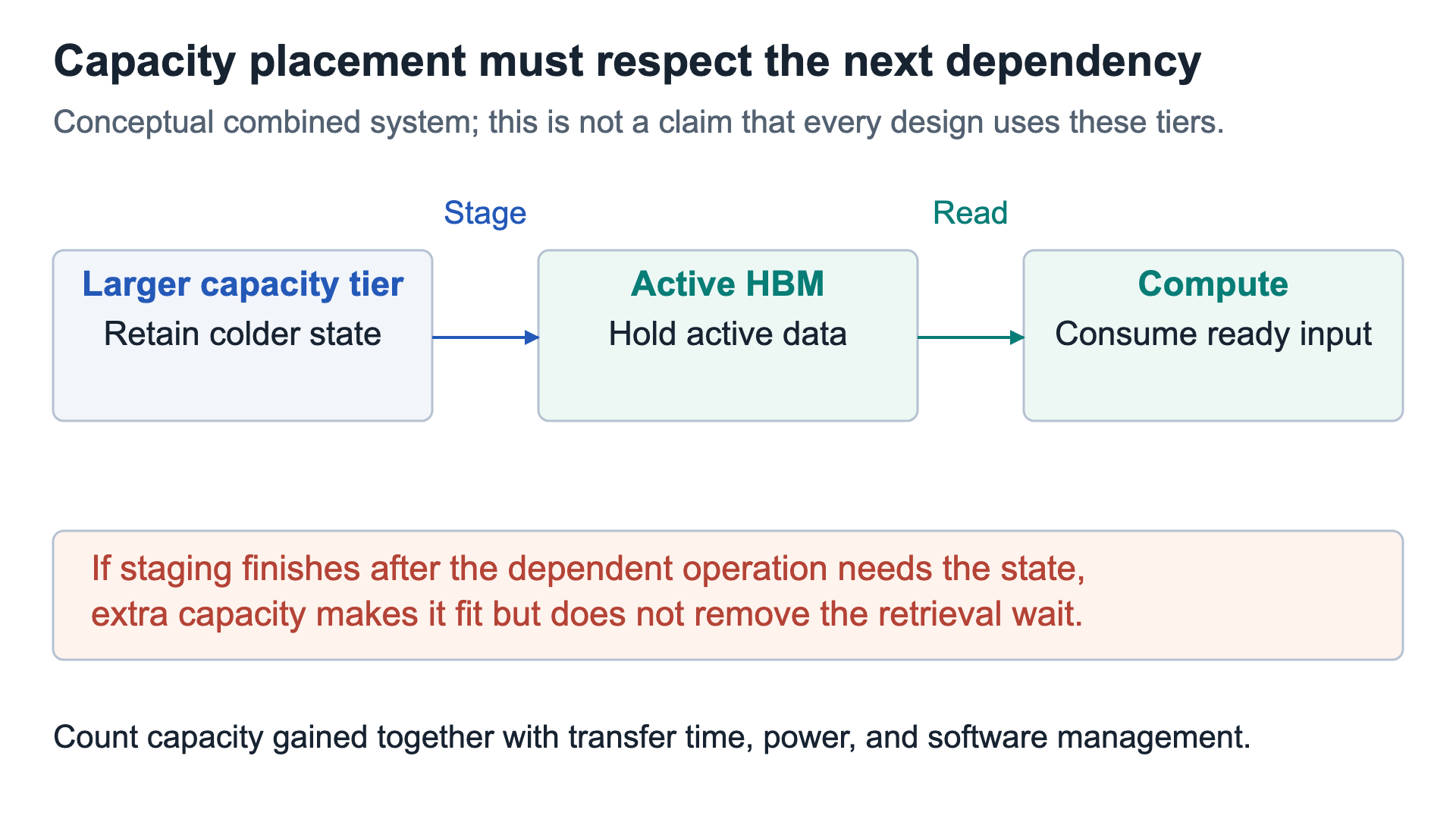
- These approaches can address different parts of one workload.
- HBM can hold the weights and KV state repeatedly needed by active requests, where the rate of delivery directly affects generation speed.
- A larger managed tier can retain colder state that would otherwise consume that scarce HBM space. Retrieving it must still finish before the dependent request needs it.
- Local computation can reduce a transfer when the memory-side hardware can turn a large input into a smaller result.
- Tighter memory integration makes component changes more interconnected. Replacing a memory stack or base die can require renewed package and thermal qualification. An already-qualified combination avoids repeating that work; substituting a part may require it again.